
Switched Mode Power Supply.
Current types of switched-mode power supply (SMPS) are commonly used and in most electronic equipment. With the advantages of high efficiency, small size, and lower cost than linear regulated power supplies with the same power. In many different types of SMPS (buck, boost, flyback, push-pull, …), the flyback power supply is widely used and has been applied in many fields. Therefore, we have researched this flyback converter.
The flyback converter is used in both AC/DC and DC/DC conversion with galvanic isolation between the input and any outputs. The flyback converter is a buck-boost converter with the inductor split to form a transformer so that the voltage ratios are multiplied with an additional advantage of isolation.

The structure of a Flyback converter includes:
- Input capacitor: filters the input voltage. The input capacitor value is also related to the time over which an input voltage can be held when input is interrupted. (Vin is a DC voltage, if the input AC voltage, it must be through the rectifier).
- RCD snubber: connects the input line and the MOSFET in the circuit diagram. The snubber circuit is inserted to suppress surge voltages, generated by leakage inductance in the transformer.
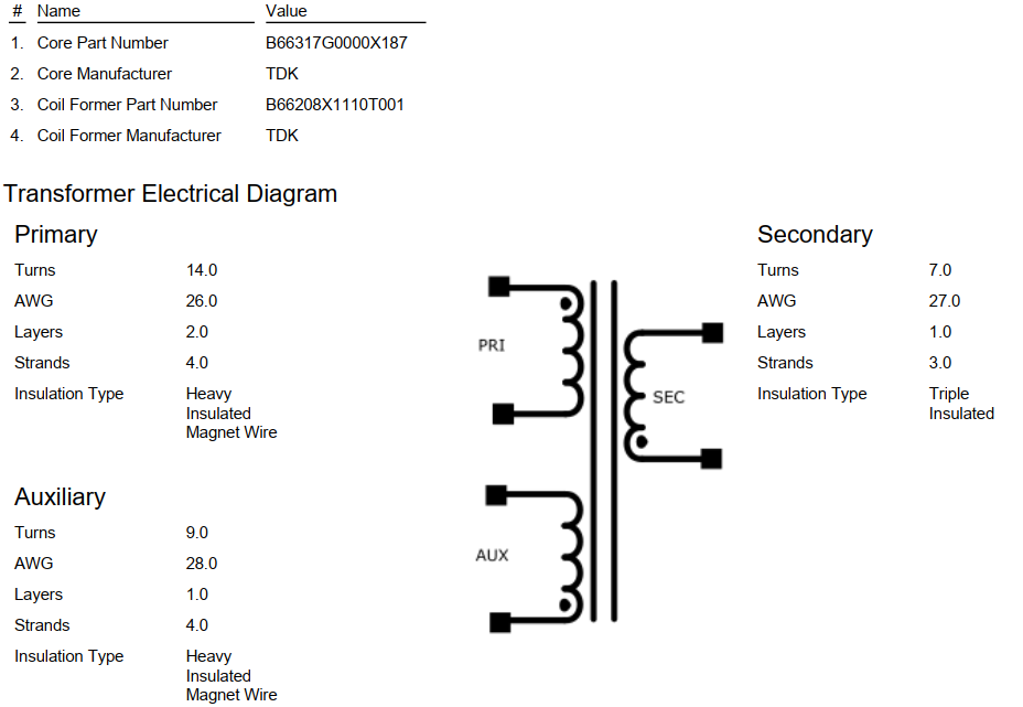
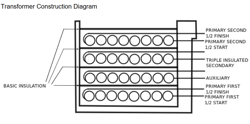
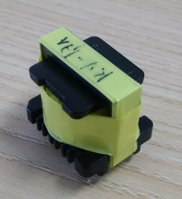
- Transformer: Voltage conversion. Input, and output voltage isolation.
- Switching element: Turn on and off according to the PWM pulse of the control IC. Often used MOSFET.
- Rectification Diode: rectifier the output voltage. Usually use types of fast switching diodes (Schottky diode, fast recovery diode).
- Output capacitor: filters the output voltage.
- Feedback loop and isolations element: the feedback output voltage, so that the circuit controls pulse width. Use Opto-isolator to isolate the output voltage from the input.
- Control IC: generate PWM pulses to control the MOSFET (BJT). Receive voltage and current feedback to adjust the pulse width.
- In addition, some circuits also add functions: overcurrent, overvoltage protection, anti-reverse polarity, …
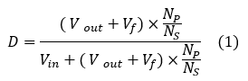
Duty cycle of Flyback converter:
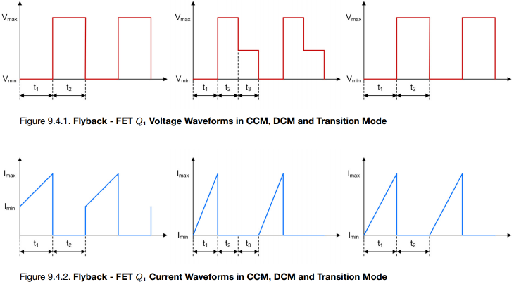
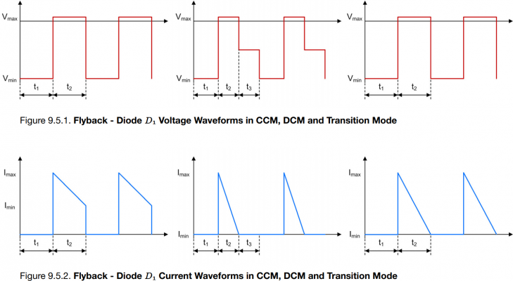
In switching operation, there are two modes:
- CCM ( Continuous Conduction Mode ).
- DCM ( Discontinuous Conduction Mode ).
CCM and DCM Waveform:

Flyback Converter Design.
We have spent a lot of time researching the DC / DC Flyback converter circuit, the input is the power source from the battery. Application for many different purposes.
Power supply specifications:
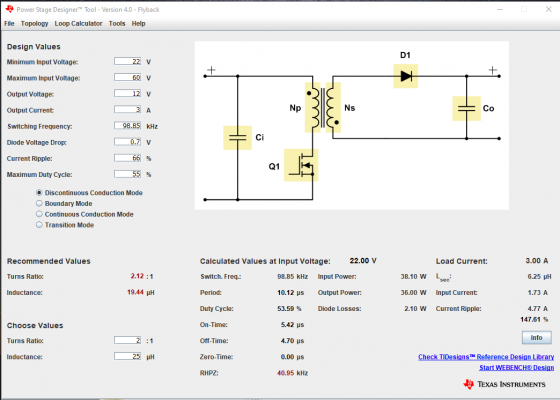
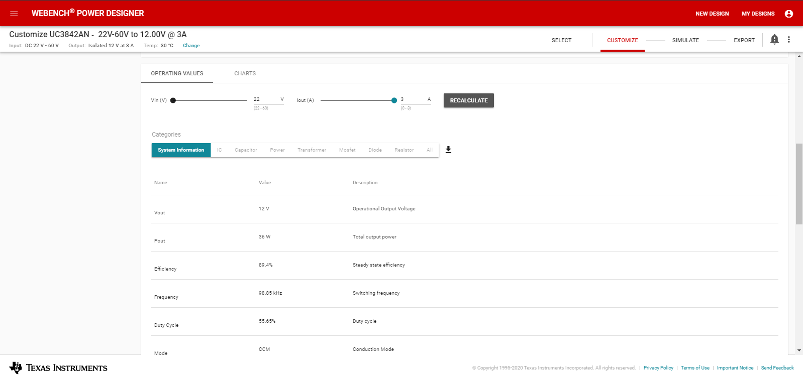
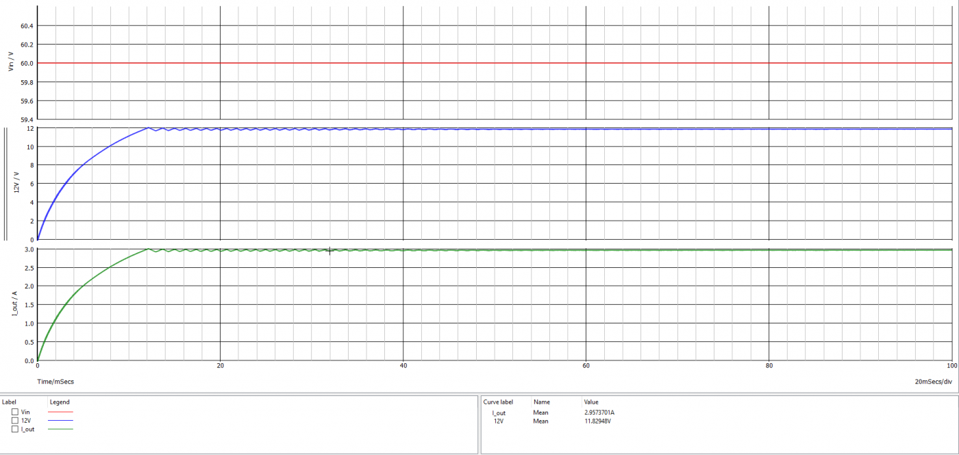
Input voltage range: +22VDC to +60VDC. Output voltage: + 12VDC. Load : 0A to 3A
In the process of researching, we used software to assist in calculating, testing, selecting components, and simulating. (Power Stage Designer, TI Webench Power Designer, SIMtrix / SIMPLIS). Refer to sample designs from manufacturers such as Texas Instruments, Analog Devices, ROHM, … to supplement and improve the design. Design the PCB and make prototypes for test measurements, and compare them with previous calculation and simulation data.
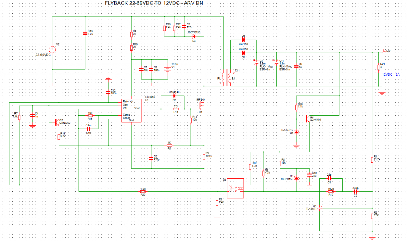
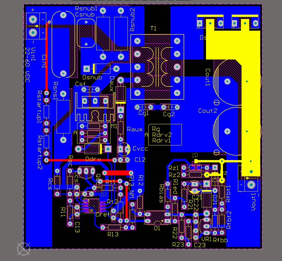
Schematic Design.
Use Texas Instruments’ Power Stage Designer Tool software to check calculated parameters.
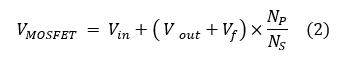
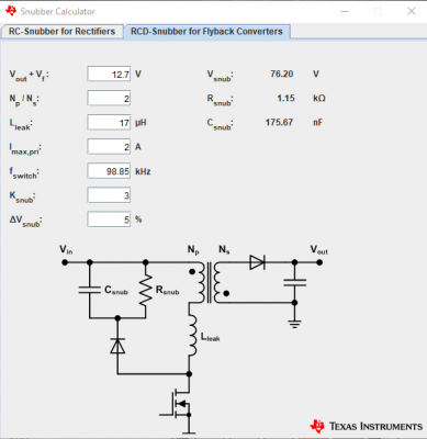
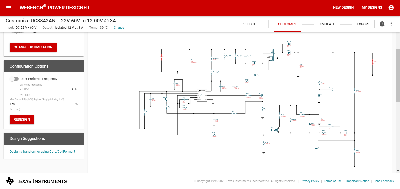
The snubber circuit, configured from a resistor, capacitor, and diode, connects the input line and the MOSFET in the circuit diagram. In the flyback design, a gap is provided in the transformer core, so that leakage magnetic flux is increased, and a leakage inductance occurs. A switching current flows in this leakage inductance as well, and energy is accumulated, but it is not coupled with the other windings, and so power is not transferred, and a surge voltage occurs across the MOSFET drain and source. When the surge voltage that occurs exceeds the MOSFET voltage rating, there is the possibility of a MOSFET failure. In order to prevent this, the snubber circuit is inserted to suppress surge voltages. One of the important components of the circuit.
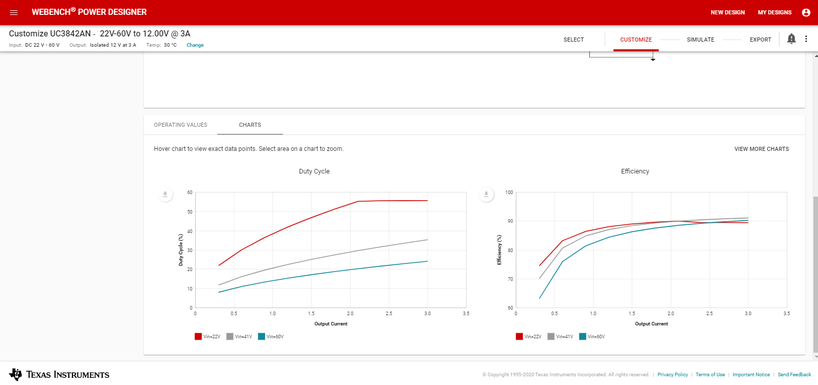
Use the Texas Instruments Webench Power Design tool to find similar designs, especially circuit specifications. In this tool, in addition to providing schematic diagrams and characteristics of each component, there are also other parameters such as voltage, current, working mode, power of the components, circuit lines, and allows to change the input value.
Simulation by SIMtrix / SIMPLIS software.
Simulate with input voltage: Vin = 22V, load : 100mA.
Simulate with input voltage: Vin = 22V, load : 3A.
Simulate with input voltage: Vin = 60V, load : 3A.
After the simulation:
- When Vin < 31VDC and Io < 2.3A, the circuit operates in DCM mode, when Io > 2.3A, it operates in CCM mode.
- When Vin > 31 VDC, the circuit only operates in DCM mode.
Comparing with data from similar designs of the maker, the values are nearly identical.
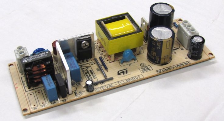
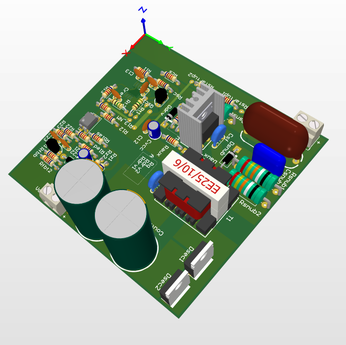
Make a Prototype And Evaluation.
After the simulation, PCB layout, and assembly.
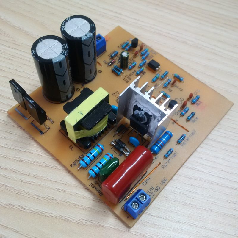
Measure and evaluate.
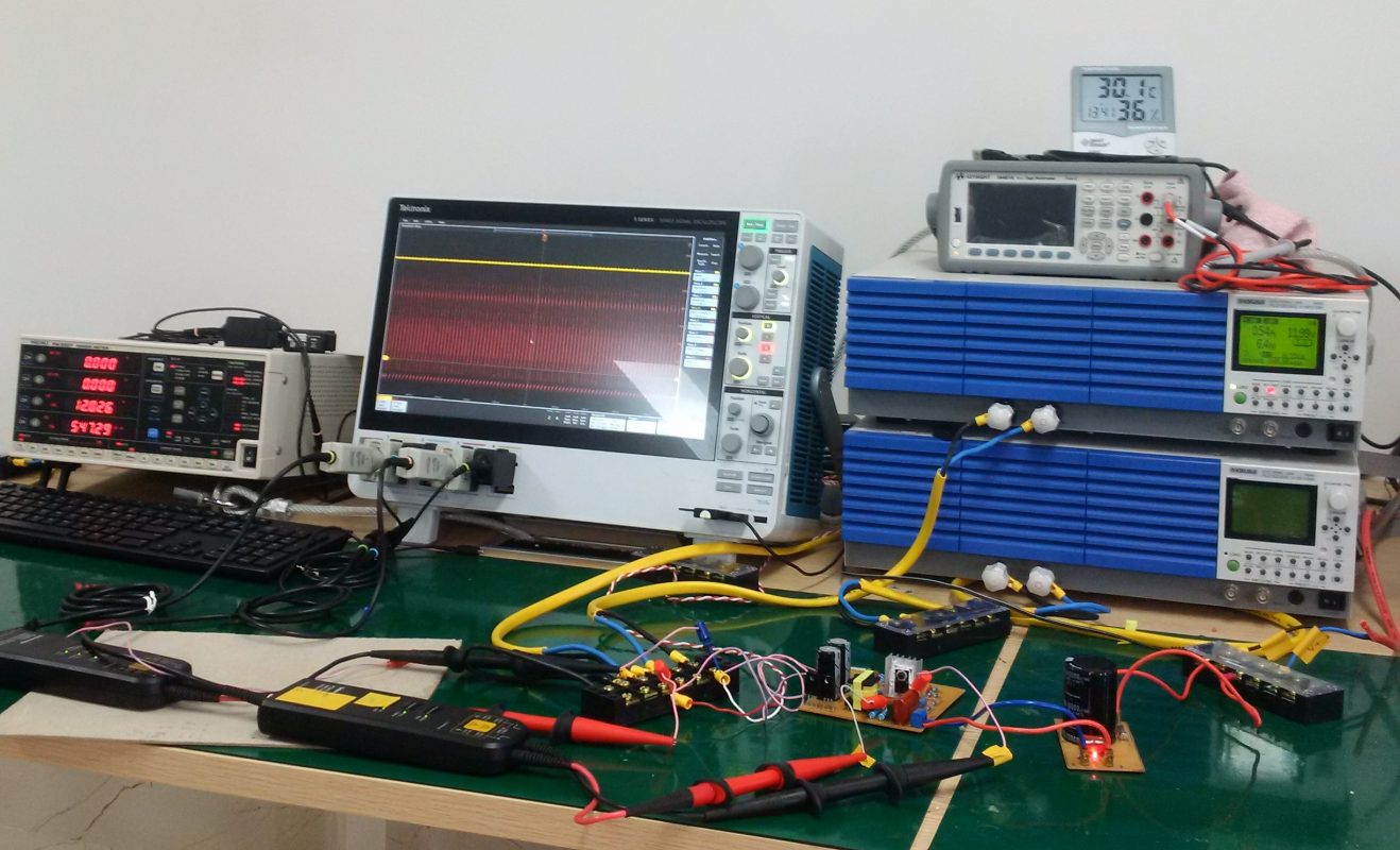
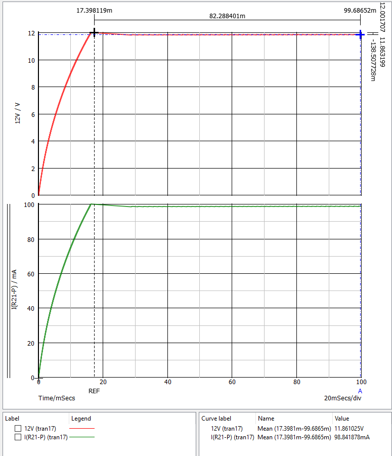
Input-Output specifications evaluation:
-
Input-Output specifications measure:
| I_out ( A ) |
Output Voltage V_out (V) |
Total output power P_out (W) |
Input Current I_in (A) |
Duty cycle D (%) |
||||||||
| Input Voltage | Input Voltage | Input Voltage | Input Voltage | |||||||||
| 22 V | 41 V | 60 V | 22 V | 41 V | 60 V | 22 V | 41 V | 60 V | 22 V | 41 V | 60 V | |
0.1 |
11.99 |
11.98 |
11.99 |
1.20 |
1.20 |
1.20 |
0.14 |
0.09 |
0.08 |
27.13% |
14.16% |
12.20% |
0.2 |
11.98 |
11.98 |
11.98 |
2.40 |
2.40 |
2.40 |
0.21 |
0.13 |
0.11 |
29.35% |
15.70% |
14.48% |
0.3 |
11.98 |
11.98 |
11.98 |
3.59 |
3.59 |
3.59 |
0.28 |
0.17 |
0.13 |
32.44% |
16.42% |
15.57% |
0.4 |
11.97 |
11.97 |
11.98 |
4.79 |
4.79 |
4.79 |
0.35 |
0.20 |
0.16 |
34.04% |
17.09% |
16.46% |
0.5 |
11.97 |
11.97 |
11.97 |
5.99 |
5.98 |
5.99 |
0.42 |
0.24 |
0.18 |
39.52% |
18.61% |
17.78% |
0.6 |
11.97 |
11.97 |
11.97 |
7.18 |
7.18 |
7.18 |
0.49 |
0.28 |
0.21 |
41.87% |
19.78% |
18.83% |
0.7 |
11.96 |
11.96 |
11.97 |
8.37 |
8.37 |
8.38 |
0.56 |
0.31 |
0.24 |
43.87% |
21.36% |
19.07% |
0.8 |
11.96 |
11.96 |
11.96 |
9.57 |
9.57 |
9.57 |
0.63 |
0.35 |
0.26 |
45.35% |
22.40% |
20.09% |
0.9 |
11.96 |
11.96 |
11.96 |
10.76 |
10.76 |
10.76 |
0.71 |
0.39 |
0.29 |
47.83% |
22.80% |
20.43% |
1.0 |
11.95 |
11.95 |
11.95 |
11.95 |
11.95 |
11.95 |
0.78 |
0.43 |
0.31 |
49.31% |
23.92% |
20.47% |
1.2 |
11.94 |
11.94 |
11.95 |
14.33 |
14.33 |
14.34 |
0.93 |
0.50 |
0.36 |
51.10% |
26.95% |
21.84% |
1.4 |
11.94 |
11.94 |
11.94 |
16.71 |
16.71 |
16.72 |
1.09 |
0.58 |
0.41 |
53.19% |
29.34% |
22.61% |
1.6 |
11.93 |
11.93 |
11.93 |
19.09 |
19.09 |
19.09 |
1.25 |
0.65 |
0.46 |
54.96% |
31.30% |
23.48% |
1.8 |
11.92 |
11.92 |
11.93 |
21.46 |
21.46 |
21.47 |
1.42 |
0.73 |
0.51 |
56.85% |
32.08% |
24.59% |
2.0 |
11.92 |
11.92 |
11.92 |
23.83 |
23.83 |
23.84 |
1.62 |
0.81 |
0.57 |
57.85% |
34.31% |
25.47% |
2.2 |
11.90 |
11.91 |
11.91 |
26.19 |
26.20 |
26.20 |
1.85 |
0.89 |
0.62 |
58.85% |
36.24% |
26.38% |
2.4 |
11.89 |
11.90 |
11.90 |
28.54 |
28.56 |
28.57 |
1.88 |
0.97 |
0.67 |
58.83% |
37.47% |
27.67% |
2.6 |
11.89 |
11.89 |
11.90 |
30.90 |
30.92 |
30.93 |
1.91 |
1.05 |
0.73 |
58.83% |
41.38% |
28.13% |
2.8 |
11.88 |
11.88 |
11.89 |
33.25 |
33.28 |
33.29 |
1.95 |
1.15 |
0.79 |
58.86% |
42.00% |
29.01% |
2.9 |
11.87 |
11.88 |
11.89 |
34.41 |
34.45 |
34.47 |
2.04 |
1.23 |
0.84 |
58.85% |
42.12% |
30.18% |
3.0 |
11.84 |
11.81 |
11.88 |
35.53 |
35.43 |
35.65 |
2.06 |
1.26 |
0.90 |
58.85% |
42.18% |
31.10% |
-
Compare the measured circuit characteristics of the circuit, with the characteristic simulated on Webench Power Design:
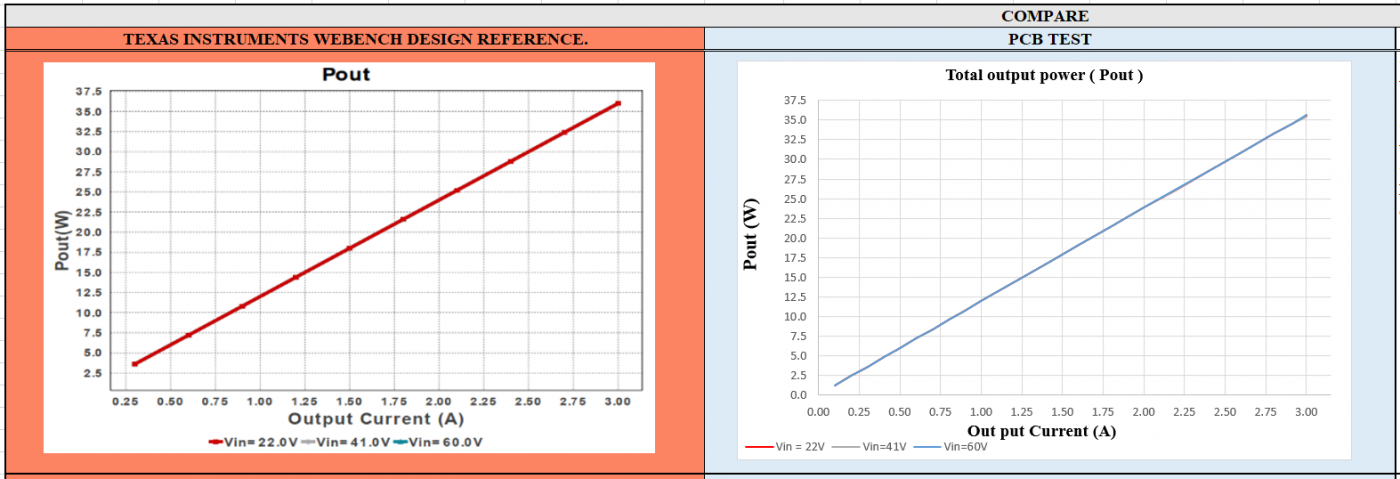
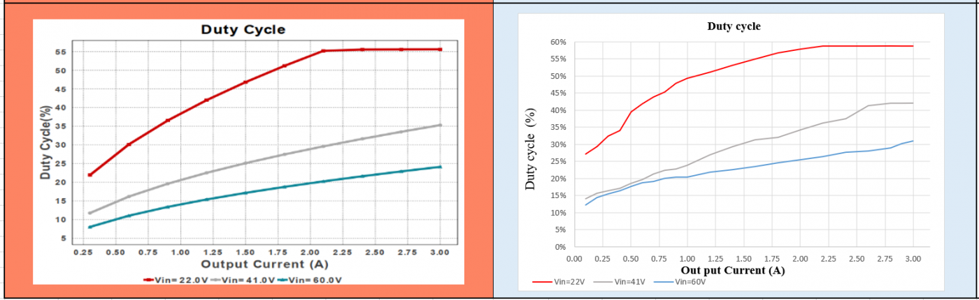
-
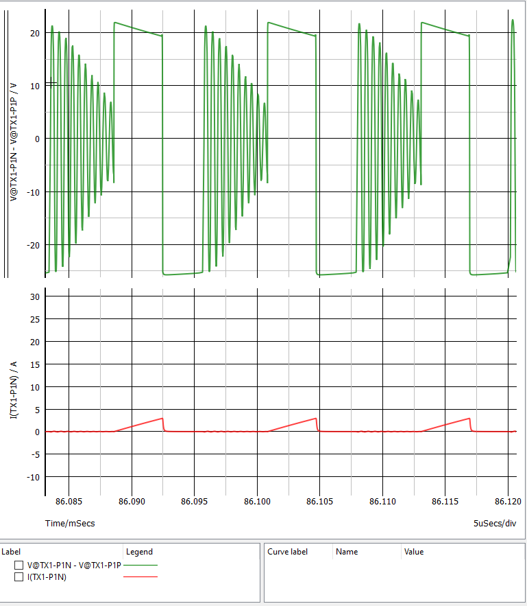
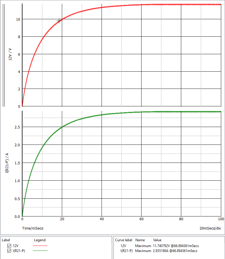
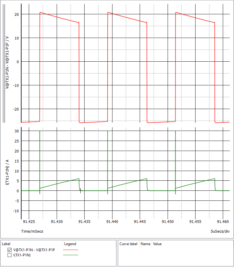
Waveform.
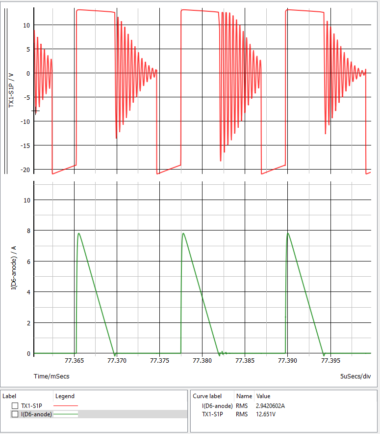
Transformer, MOSFET, and rectification Diode specifications evaluation:
-
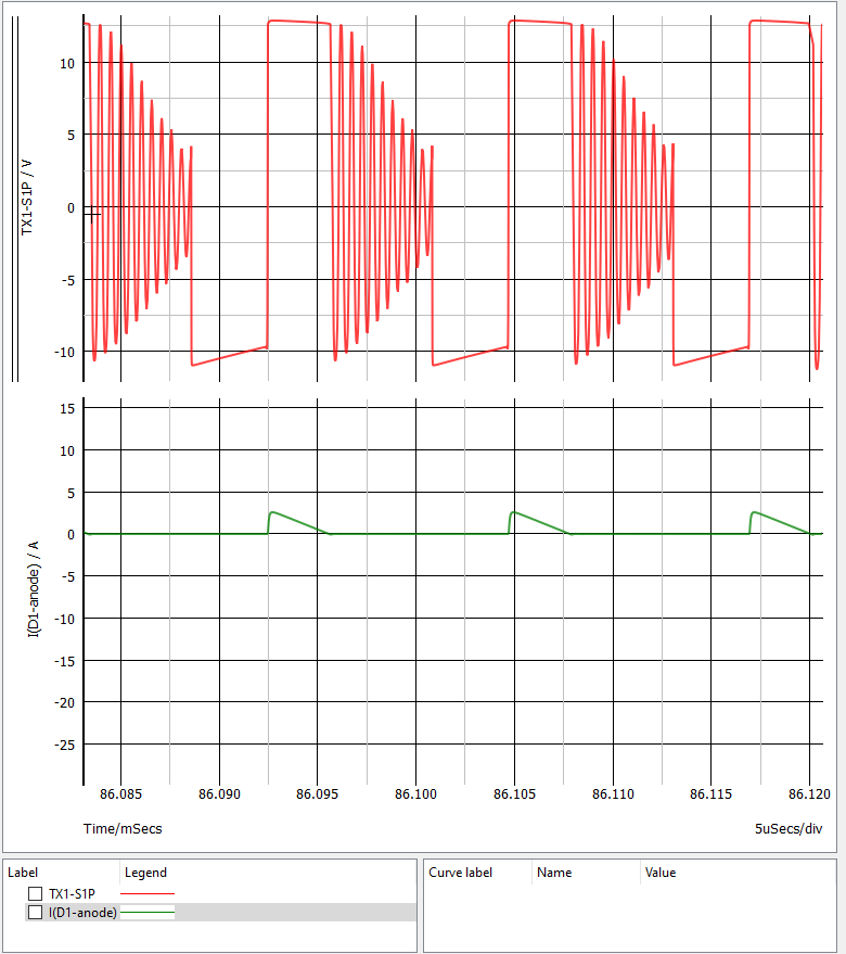
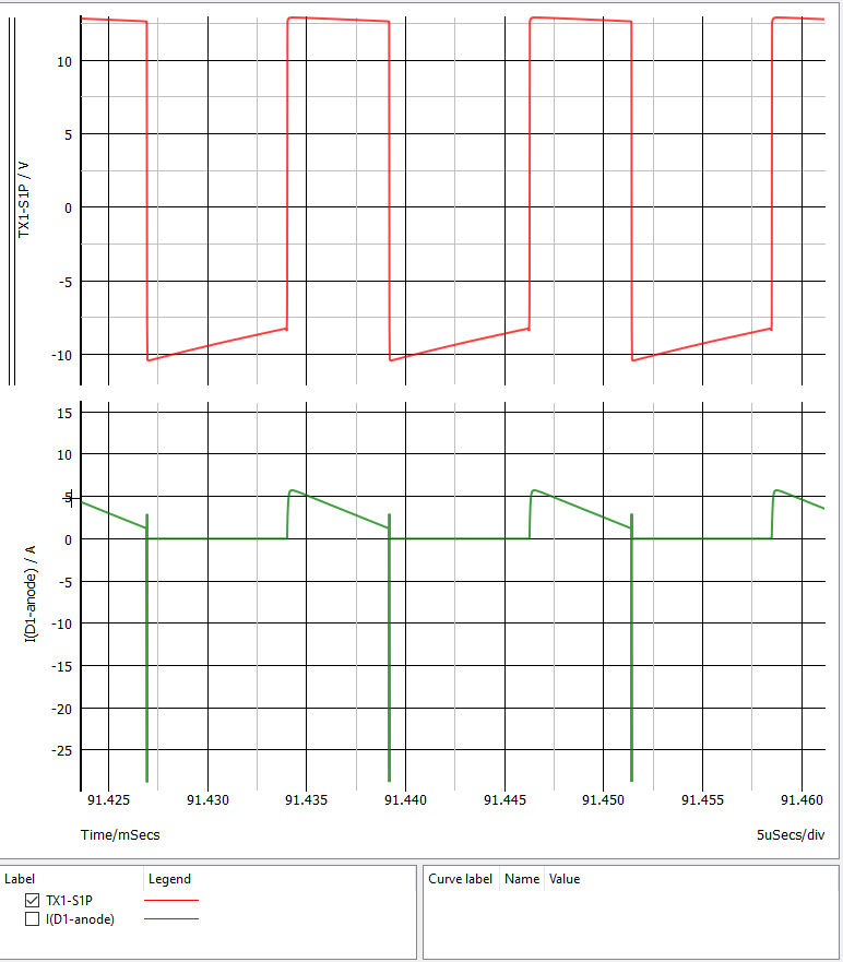
Rectification Diode voltage and current measure:
| Iout ( A ) | Dsec If | Dsec Vf | Dsec Pd | Dsec If | Dsec Vf | Dsec Pd | Dsec If | Dsec Vf | Dsec Pd |
| 0.1 | 0.12237 | 0.58 | 0.070975 | 0.14025 | 0.585 | 0.082046 | 0.1581 | 0.33 | 0.052173 |
| 0.2 | 0.2229 | 0.6 | 0.13374 | 0.2375 | 0.595 | 0.141313 | 0.2542 | 0.35 | 0.08897 |
| 0.3 | 0.3214 | 0.605 | 0.194447 | 0.3367 | 0.61 | 0.205387 | 0.3538 | 0.35 | 0.12383 |
| 0.4 | 0.4166 | 0.62 | 0.258292 | 0.4359 | 0.61 | 0.265899 | 0.4529 | 0.36 | 0.163044 |
| 0.5 | 0.5179 | 0.62 | 0.321098 | 0.5368 | 0.61 | 0.327448 | 0.5506 | 0.35 | 0.19271 |
| 0.6 | 0.6207 | 0.63 | 0.391041 | 0.6332 | 0.61 | 0.386252 | 0.6486 | 0.365 | 0.236739 |
| 0.7 | 0.7182 | 0.63 | 0.452466 | 0.736 | 0.635 | 0.46736 | 0.7483 | 0.375 | 0.280612 |
| 0.8 | 0.8185 | 0.66 | 0.54021 | 0.8336 | 0.65 | 0.54184 | 0.8508 | 0.385 | 0.327558 |
| 0.9 | 0.9216 | 0.645 | 0.594432 | 0.9315 | 0.64 | 0.59616 | 0.948 | 0.385 | 0.36498 |
| 1 | 1.0257 | 0.67 | 0.687219 | 1.0334 | 0.635 | 0.656209 | 1.0518 | 0.4 | 0.42072 |
| 1.2 | 1.2232 | 0.685 | 0.837892 | 1.2292 | 0.65 | 0.79898 | 1.2453 | 0.42 | 0.523026 |
| 1.4 | 1.4241 | 0.715 | 1.018232 | 1.4283 | 0.66 | 0.942678 | 1.4446 | 0.43 | 0.621178 |
| 1.6 | 1.6212 | 0.71 | 1.151052 | 1.6295 | 0.67 | 1.091765 | 1.6451 | 0.46 | 0.756746 |
| 1.8 | 1.8732 | 0.75 | 1.4049 | 1.8336 | 0.68 | 1.246848 | 1.8433 | 0.47 | 0.866351 |
| 2 | 2.069 | 0.725 | 1.500025 | 2.0319 | 0.69 | 1.402011 | 2.0423 | 0.485 | 0.990515 |
| 2.2 | 2.272 | 0.755 | 1.71536 | 2.274 | 0.7 | 1.5918 | 2.285 | 0.51 | 1.16535 |
| 2.4 | 2.473 | 0.775 | 1.916575 | 2.472 | 0.72 | 1.77984 | 2.482 | 0.51 | 1.26582 |
| 2.6 | 2.669 | 0.776 | 2.071144 | 2.669 | 0.73 | 1.94837 | 2.684 | 0.54 | 1.44936 |
| 2.8 | 2.873 | 0.774 | 2.223702 | 2.871 | 0.725 | 2.081475 | 2.884 | 0.565 | 1.62946 |
| 2.9 | 2.965 | 0.778 | 2.30677 | 2.973 | 0.74 | 2.20002 | 2.983 | 0.575 | 1.715225 |
| 3 | 3.043 | 0.782 | 2.379626 | 3.073 | 0.76 | 2.33548 | 3.086 | 0.585 | 1.80531 |
- Compare the measured circuit characteristics of the circuit, with the characteristic simulated on Webench Power Design:
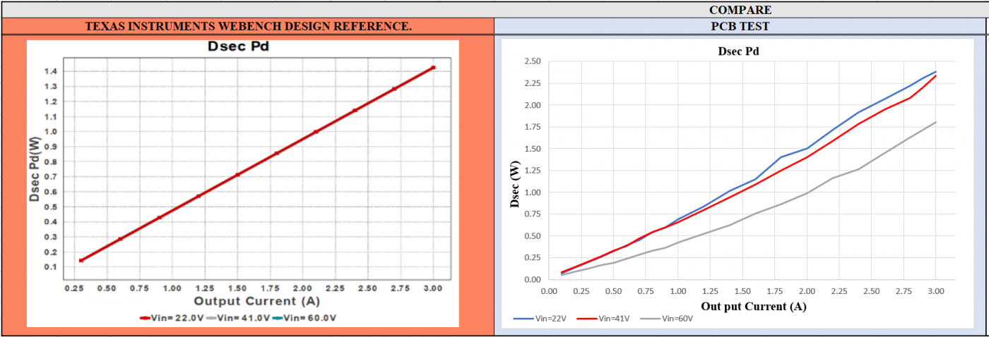
- Waveform.
-
-
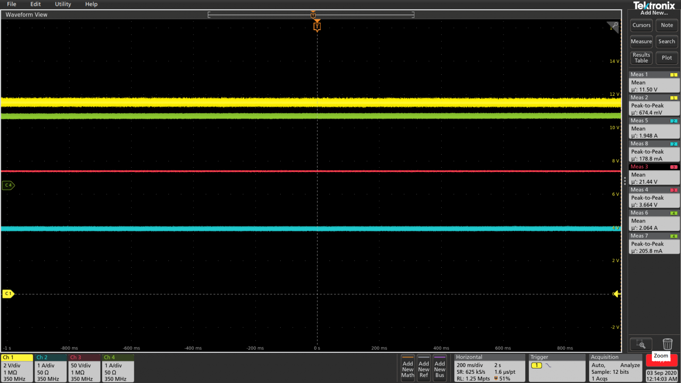
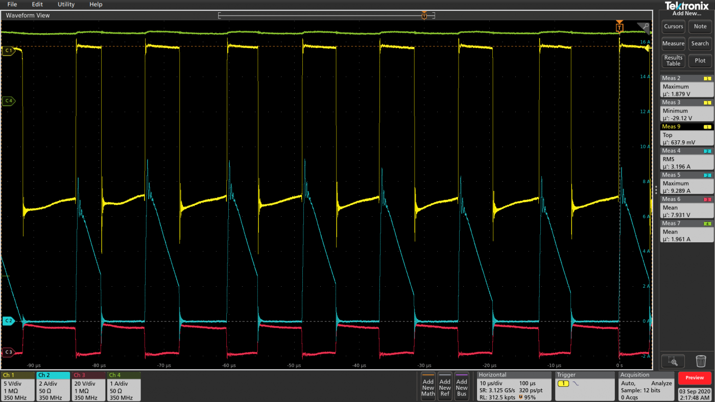
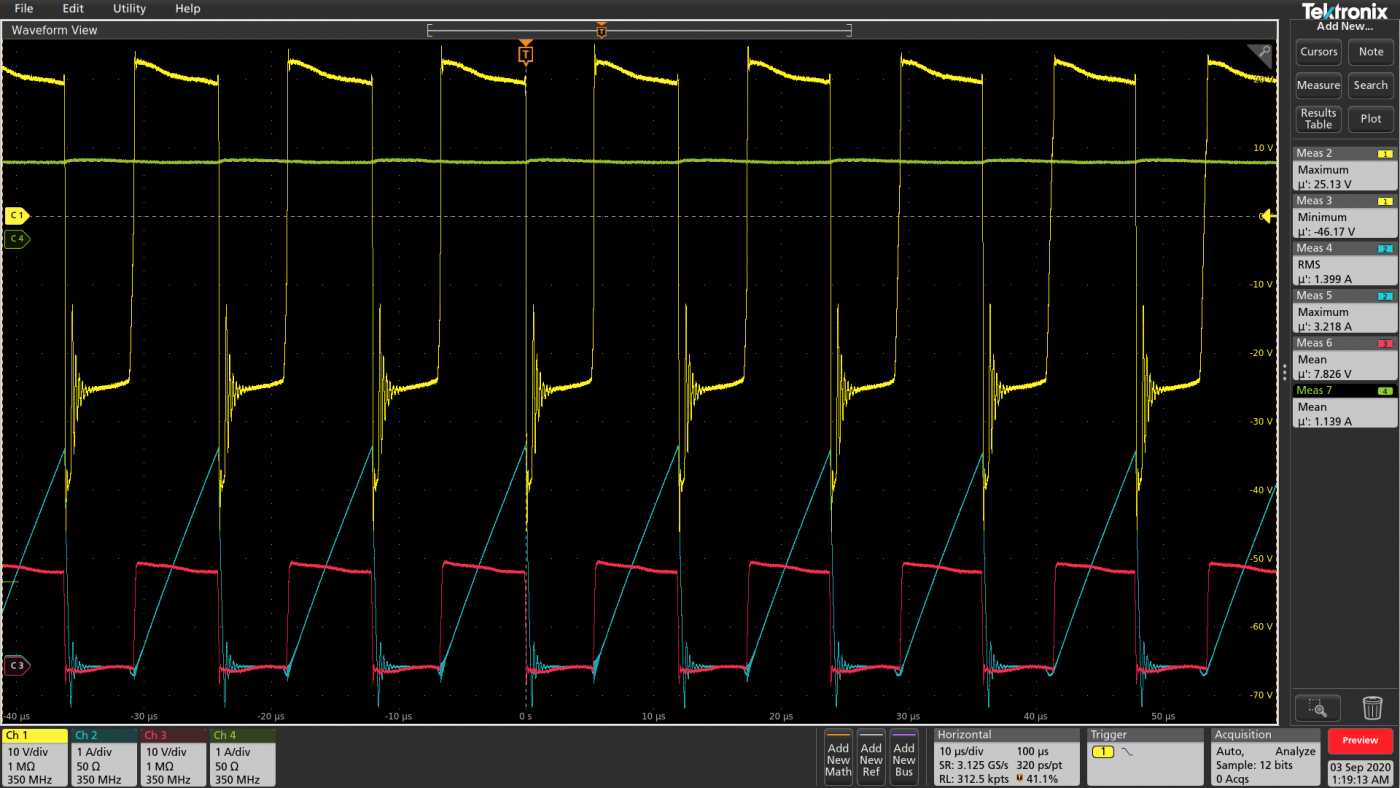
Evaluation with input voltage: Vin = 22V, load Io = 1.1 A. The circuit operates in DCM mode:
-
-
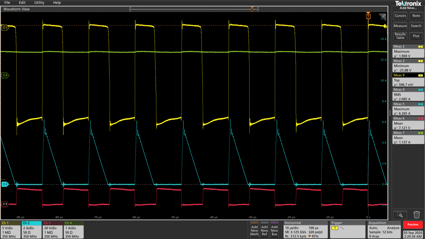
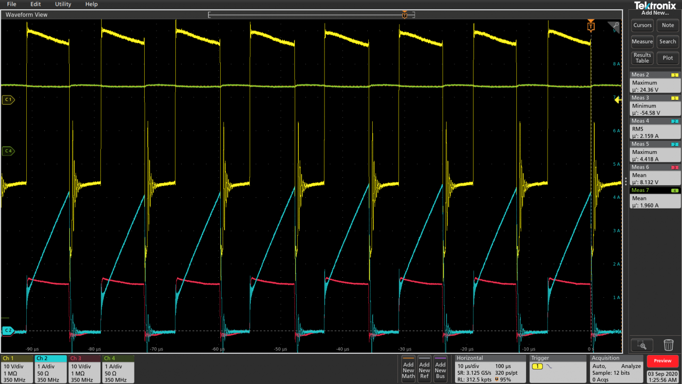
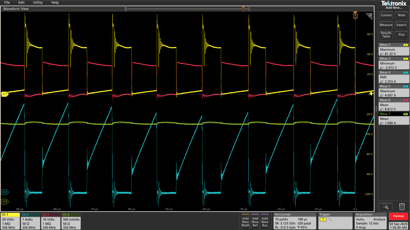
- Evaluation with input voltage: Vin = 22V, load Io = 1.961 A. The circuit operates in CCM mode:
-
-
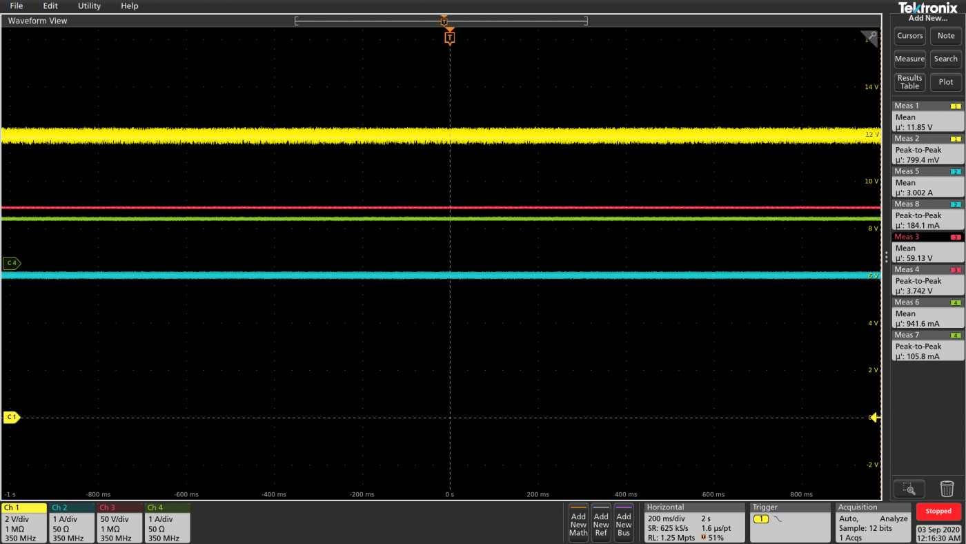
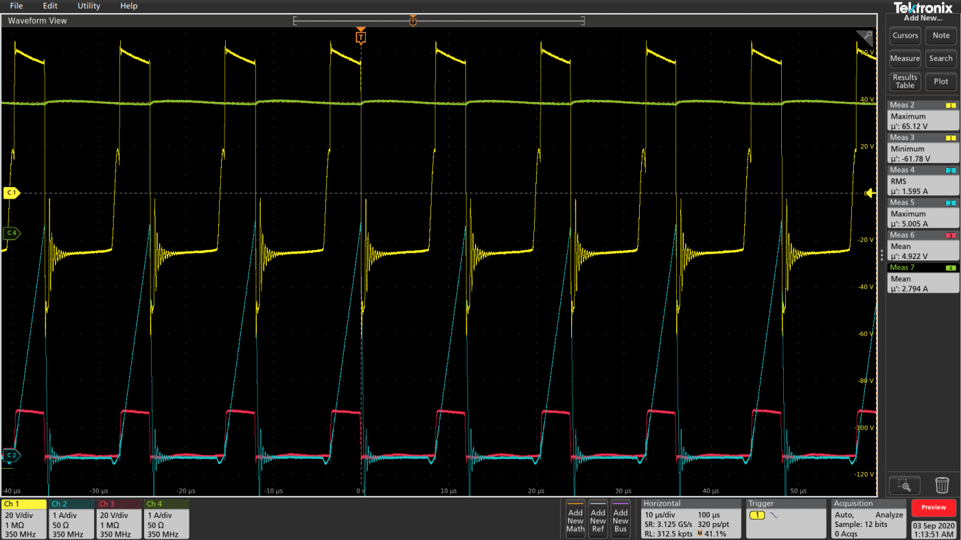
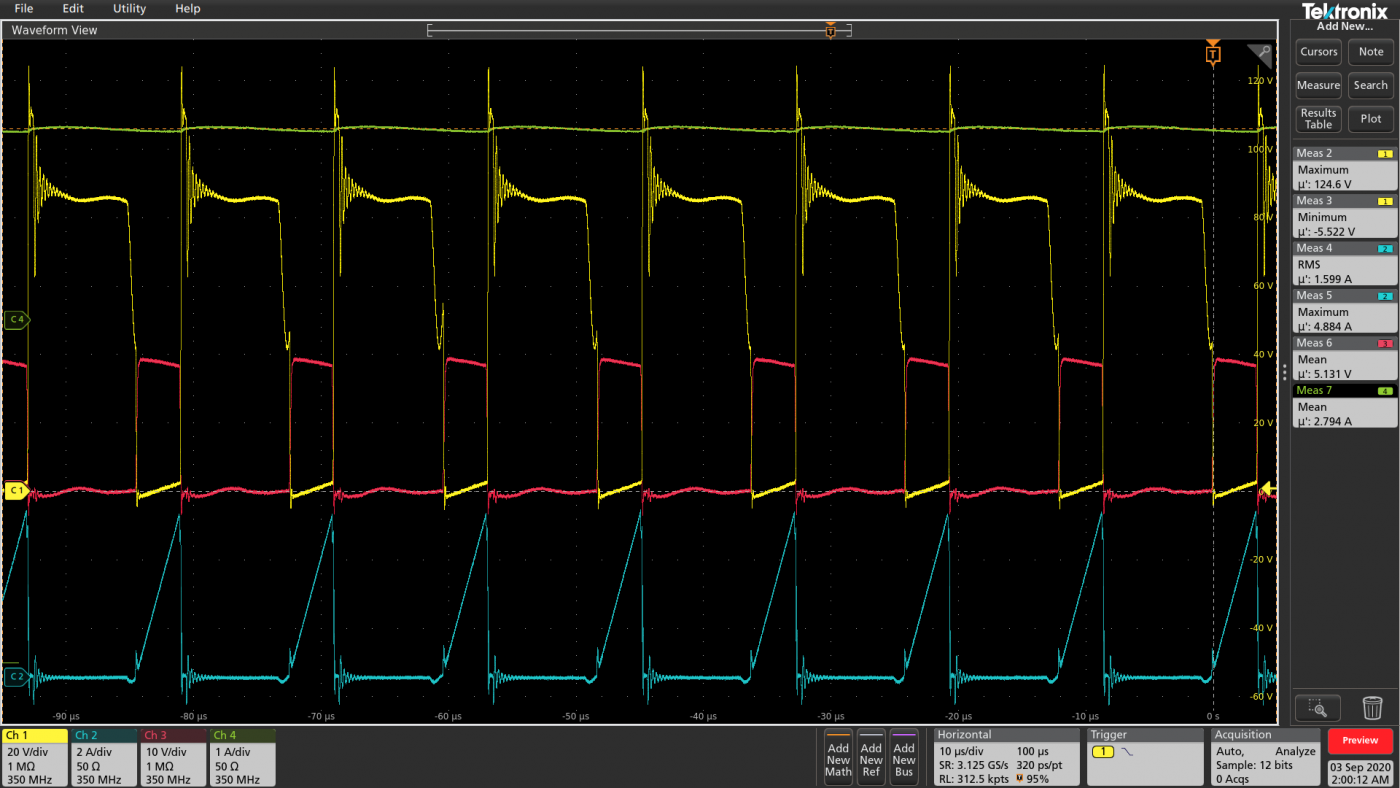
Evaluation with input voltage: Vin = 60V, load Io = 2.8 A. The circuit operates in DCM mode:
-

-
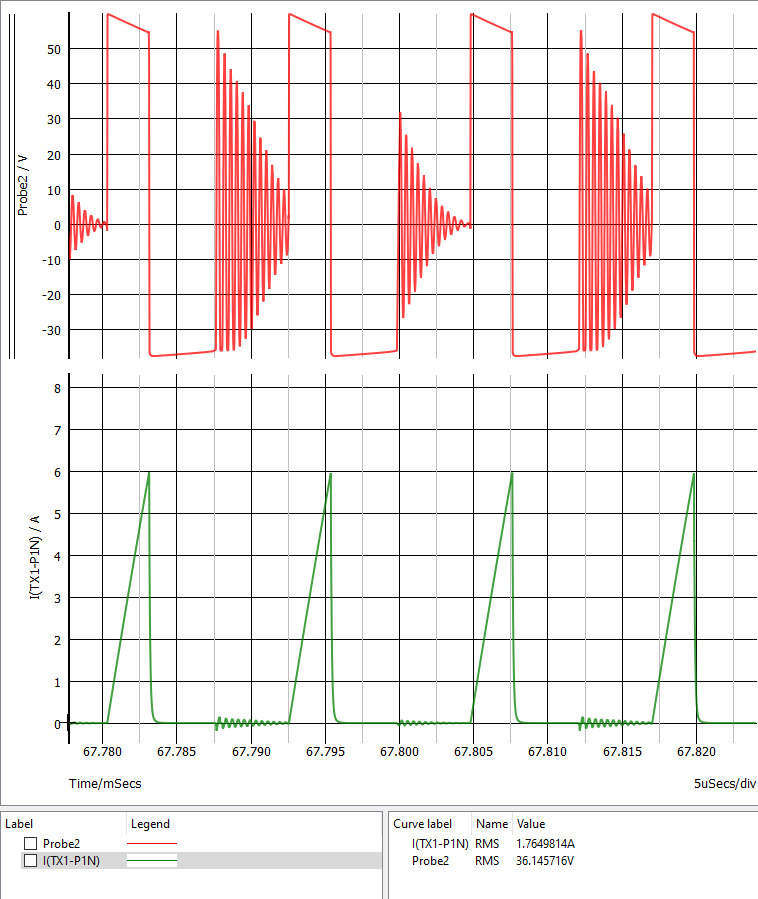
Primary RMS current, and Secondary winding RMS current measure:
| Iout ( A ) | Primary RMS Current T1 Iprim RMS (A) |
Secondary1 Winding RMS Current T1 Is1 RMS (A) |
||||
| Input Voltage | Input Voltage | |||||
| 22 V | 41 V | 60 V | 22 V | 41 V | 60 V | |
| 0.1 | 0.3682 | 0.3331 | 0.3216 | 0.3902 | 0.4102 | 0.4802 |
| 0.2 | 0.4622 | 0.4235 | 0.3928 | 0.5887 | 0.5661 | 0.5312 |
| 0.3 | 0.5208 | 0.5060 | 0.4570 | 0.7205 | 0.7331 | 0.7370 |
| 0.4 | 0.6202 | 0.5753 | 0.5236 | 0.8983 | 0.8250 | 0.9550 |
| 0.5 | 0.7161 | 0.6177 | 0.5700 | 1.0700 | 1.0400 | 1.1030 |
| 0.6 | 0.8114 | 0.6636 | 0.6165 | 1.2350 | 1.1520 | 1.3370 |
| 0.7 | 0.9072 | 0.7339 | 0.6813 | 1.3960 | 1.2880 | 1.5330 |
| 0.8 | 0.9983 | 0.8025 | 0.7405 | 1.5650 | 1.4270 | 1.6720 |
| 0.9 | 1.0900 | 0.8663 | 0.7992 | 1.7170 | 1.5330 | 1.8540 |
| 1.0 | 1.1800 | 0.9312 | 0.8035 | 1.8630 | 1.6860 | 1.9820 |
| 1.2 | 1.3500 | 1.0610 | 0.8571 | 2.1420 | 1.9510 | 2.2500 |
| 1.4 | 1.5230 | 1.1870 | 0.9545 | 2.4130 | 2.2060 | 2.5200 |
| 1.6 | 1.7050 | 1.3040 | 1.0460 | 2.6960 | 2.4520 | 2.7760 |
| 1.8 | 1.9120 | 1.4190 | 1.1380 | 2.9910 | 2.6870 | 3.0220 |
| 2.0 | 2.1440 | 1.5370 | 1.2260 | 3.3080 | 2.9260 | 3.2640 |
| 2.2 | 2.4040 | 1.6460 | 1.3060 | 3.8410 | 3.1490 | 3.4910 |
| 2.4 | 2.7150 | 1.7570 | 1.3960 | 4.1552 | 3.3710 | 3.7210 |
| 2.6 | 2.8151 | 1.8780 | 1.4830 | 4.4338 | 3.5960 | 3.9460 |
| 2.8 | 2.9292 | 1.9820 | 1.5630 | 4.7825 | 3.8010 | 4.2100 |
| 2.9 | 3.0192 | 2.0890 | 1.6790 | 4.9530 | 3.9320 | 4.3190 |
| 3.0 | 3.1256 | 2.1920 | 1.7490 | 5.1254 | 4.0000 | 4.4550 |
- Compare the measured circuit characteristics of the circuit, with the characteristic simulated on Webench Power Design:
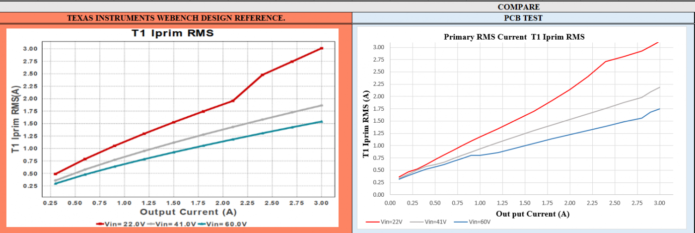
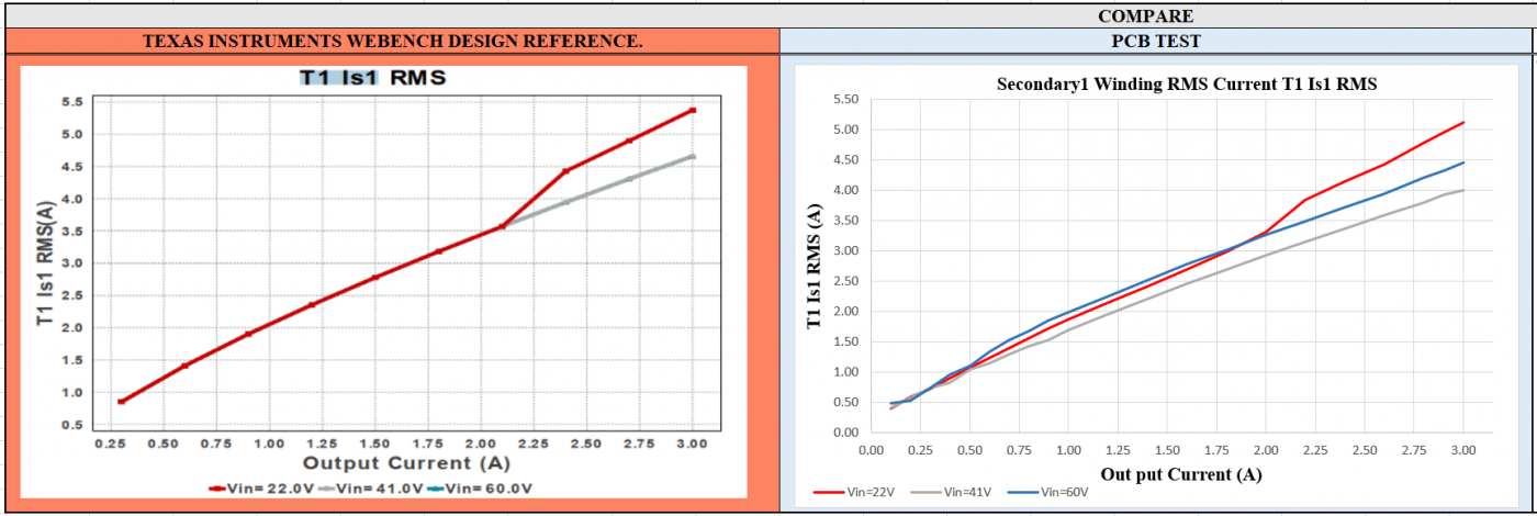
- Waveform.
-
-
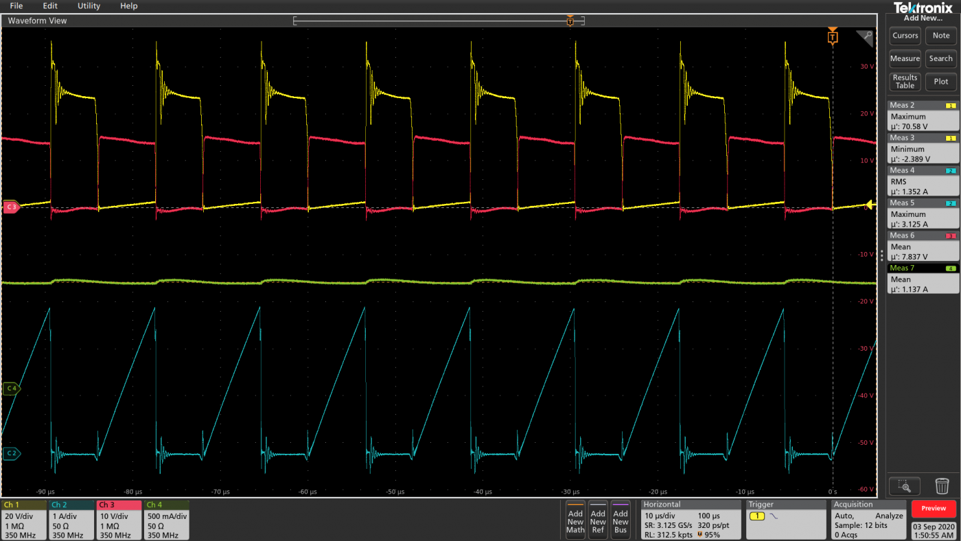
Evaluation with input voltage: Vin = 22V, load Io = 1.1 A. The circuit operates in DCM mode:
-
-
-
Evaluation with input voltage: Vin = 22V, load Io = 1.961 A. The circuit operates in CCM mode:
-
-
-
Evaluation with input voltage: Vin = 60V, load Io = 2.8 A. The circuit operates in DCM mode:
-
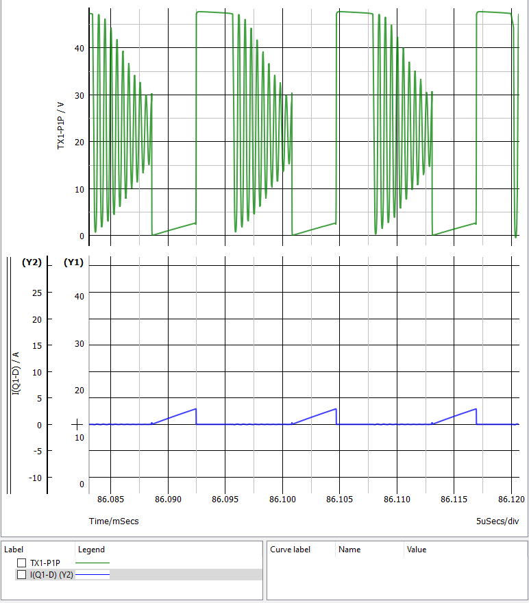
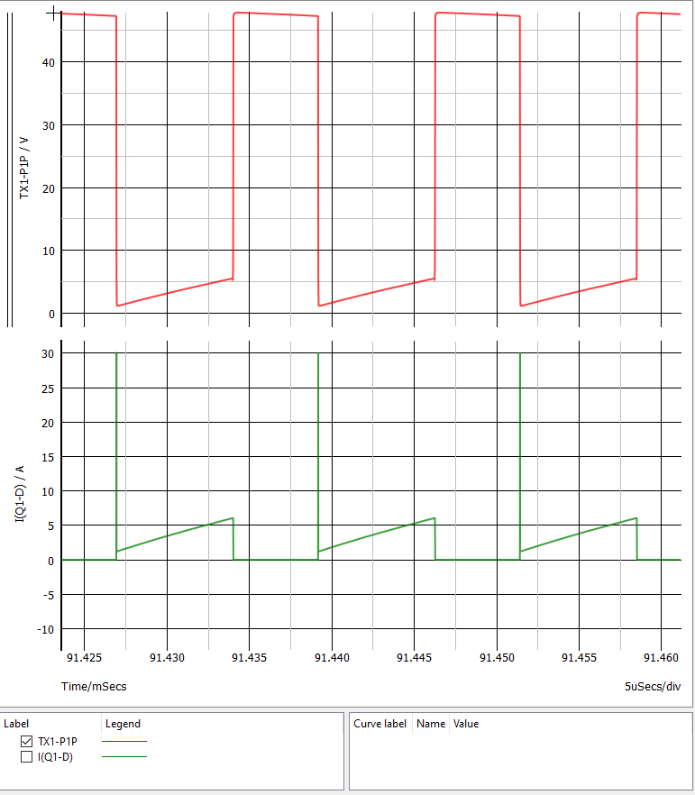
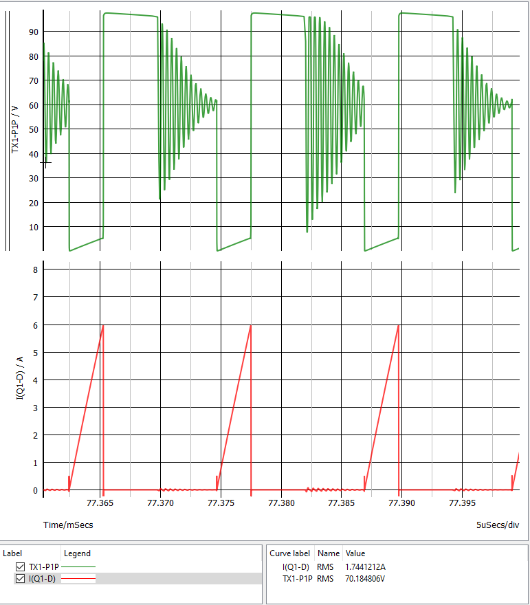
MOSFET specifications evaluation:
-
Waveform.
-
Evaluation with input voltage: Vin = 22V, load Io = 1.1 A. The circuit operates in DCM mode:
-
-
-
Evaluation with input voltage: Vin = 22V, load Io = 1.961 A. The circuit operates in CCM mode:
-
-
-
Evaluation with input voltage: Vin = 60V, load Io = 2.8 A. The circuit operates in DCM mode:
-
In the process of researching, it is inevitable that there are shortcomings, we hope to receive comments from readers, helping us to improve.
ARD-DN Team
References:
Markus Zehendner, Matthias Ulmann, “Power Topologies Handbook “, Texas Instruments.
“Under the Hood of Flyback SMPS Designs”, TI Literature Number: SLUP254,Texas Instruments.
“Methods of Designing PWM Flyback Converter”, Rohm Semiconductor.
“Design Guidelines for RCD Snubber of Flyback Converters”, Application Note AN-4147, Fairchild Semiconductor.
“DC-DC Converters Feedback and Control”, Application Note TND352, ON Semiconductor
https://webench.ti.com/power-designer/switching-regulator