
Switched Mode Power Supply.
現在のスイッチング電源(SMPS: switched-mode power supply)は、ほとんどの電子機器に一般的に使用されている。同じ電力を供給するリニア安定化電源に比べ、高効率、小型、低コストという利点がある。多くの異なるタイプのSMPS(降圧、昇圧、フライバック、プッシュプル、…)の中で、フライバック電源は広く使用されており、多くの分野で応用されている。そこで、このフライバック・コンバータを研究した。
フライバック・コンバータは、入力と出力の間をガルバニック絶縁したAC/DC変換とDC/DC変換の両方に使用される。フライバック・コンバータは、インダクタを分割してトランスを形成した降圧コンバータであるため、電圧比で乗算され、さらに絶縁という利点がある。

フライバックコンバータの構造:
- 入力コンデンサー:入力電圧を平滑化する。入力コンデンサの値は、入力が遮断されたときに入力電圧を保持できる時間にも関係する。(Vinは直流電圧で、入力が交流電圧の場合は整流器を通す必要がある)。
- RCDスナバ:回路図の入力ラインとMOSFETを接続する。スナバ回路は、トランスの漏れインダクタンスによって発生するサージ電圧を抑制するために挿入される。
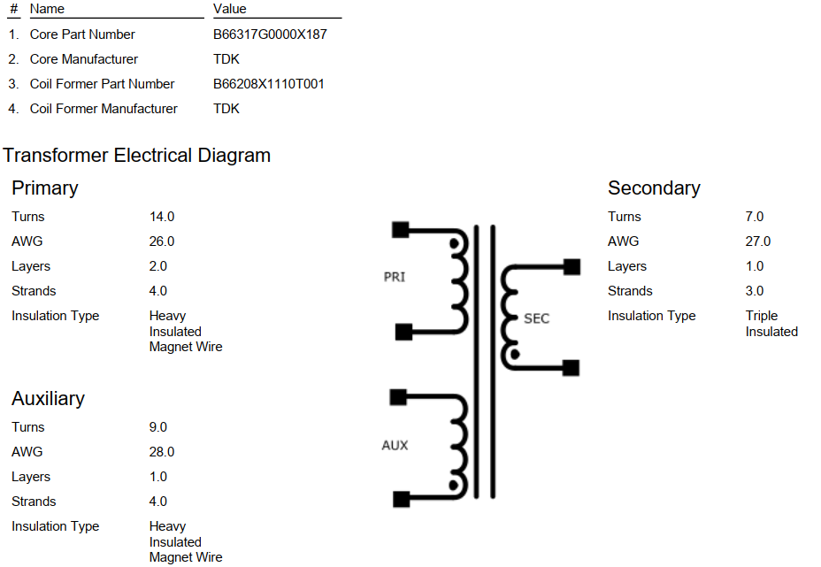
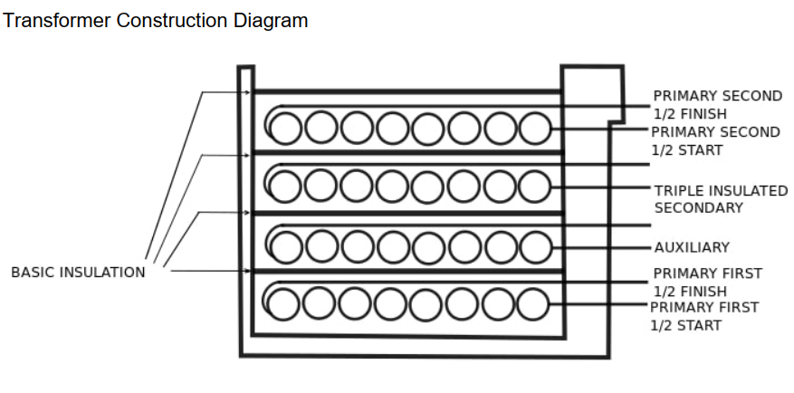
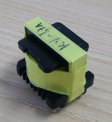
- トランス: 電圧変換。入力電圧と出力電圧の絶縁。
- スイッチング素子: 制御ICのPWMパルスに従ってオン・オフする。MOSFETがよく使われる。
- 整流ダイオード:出力電圧を整流する。通常、高速スイッチング・ダイオード(ショットキー・ダイオード、ファストリカバリー・ダイオード)を使用する。
- 出力コンデンサ:出力電圧をフィルタリングする。
- フィードバックループと絶縁素子:回路がパルス幅を制御するように、出力電圧をフィードバックする。オプトアイソレーターを使用して、出力電圧を入力から絶縁する。
- 制御IC:MOSFET(BJT)を制御するためにPWMパルスを生成する。電圧と電流のフィードバックを受けてパルス幅を調整する。
さらに、過電流、過電圧保護、逆極性防止などの機能を追加する回路もある。
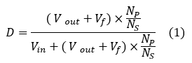
フライバックコンバータのデューティサイクル:
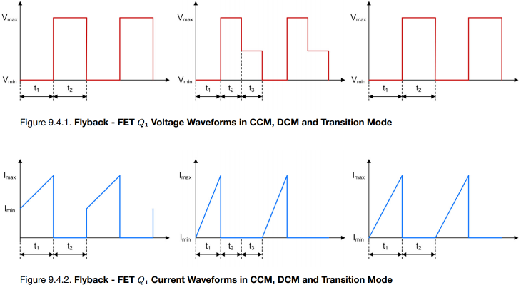
スイッチング動作の2つのモード:
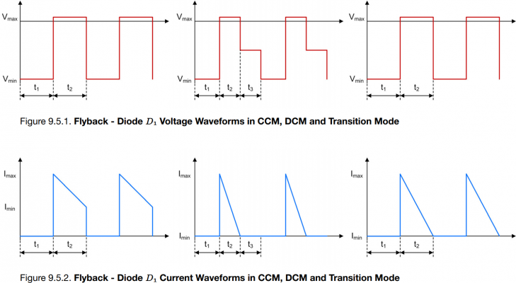
- CCM ( Continuous Conduction Mode ).
- DCM ( Discontinuous Conduction Mode ).
CCM and DCM Waveform:

フライバックコンバータの設計.
DC/DCフライバックコンバータ回路は様々な用途に使用できる。
電源電圧設計:
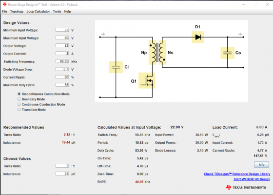
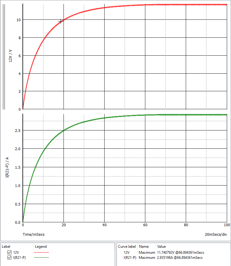
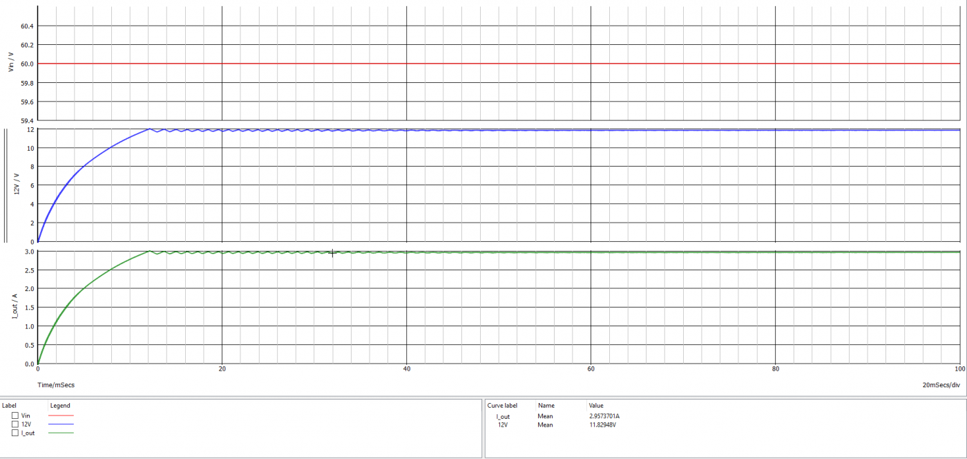
Input voltage range: +22VDC to +60VDC. Output voltage: + 12VDC. Load : 0A to 3A
研究の過程で、計算、テスト、部品の選択、シミュレーションを支援するソフトウェアを使用した。(Power Stage Designer、TI Webench Power Designer、SIMtrix / SIMPLIS)。テキサス・インスツルメンツ、アナログ・デバイセズ、ロームなどのメーカーのサンプル設計を参照し、設計を補足・改善した。PCBを設計し、テスト測定用のプロトタイプを作成し、以前の計算およびシミュレーション・データと比較した。
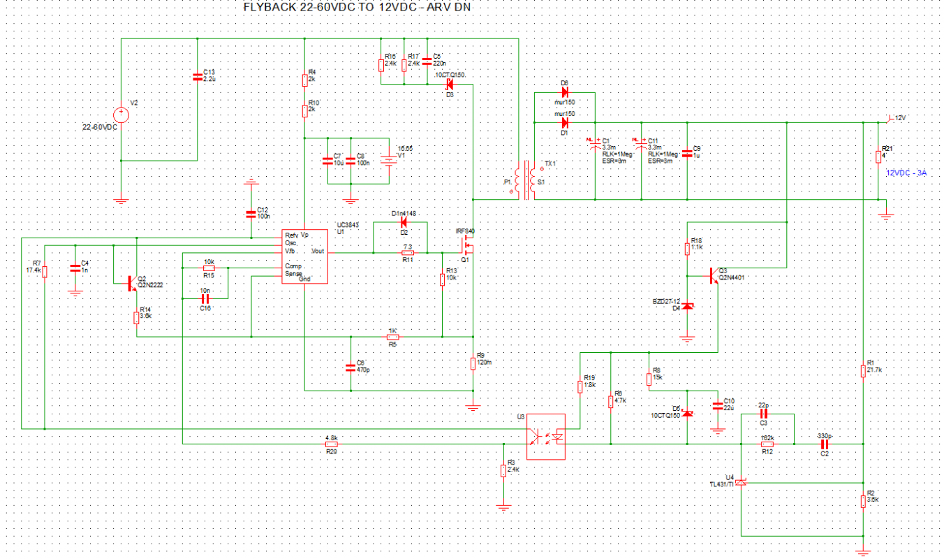
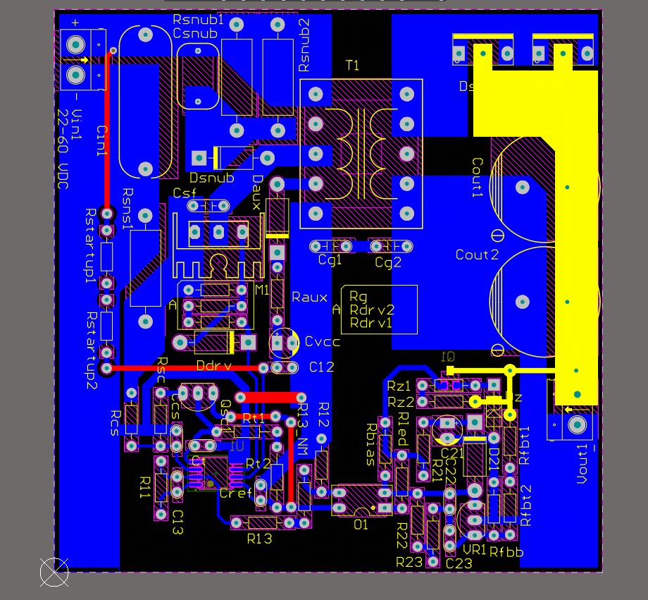
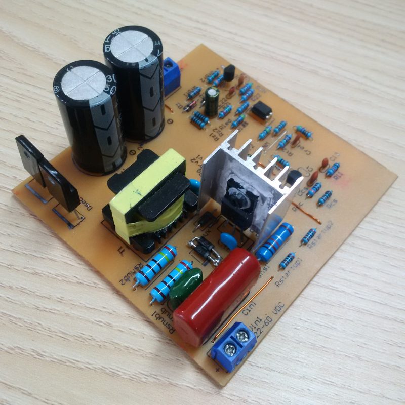
回路設計.
計算されたパラメータを確認するために、テキサス・インスツルメンツのPower Stage Designer Toolソフトウェアを使用した。
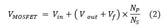
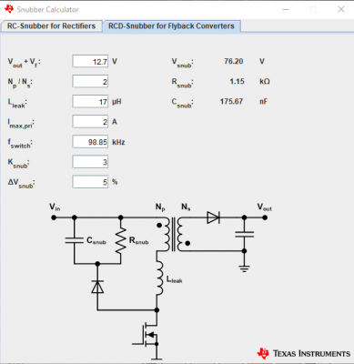
抵抗、コンデンサ、ダイオードで構成されるスナバ回路は、回路図では入力ラインとMOSFETに接続されている。フライバック設計では、トランスコアにギャップが設けられるため、漏れ磁束が増加し、漏れインダクタンスが発生する。この漏れインダクタンスにもスイッチング電流が流れ、エネルギーが蓄積されるが、他の巻線とは結合されないため電力は伝達されず、MOSFETのドレインとソースにサージ電圧が発生する。発生したサージ電圧がMOSFETの定格電圧を超えると、MOSFETが故障する可能性がある。これを防ぐため、スナバ回路を挿入してサージ電圧を抑制する。この回路の重要な構成要素のひとつである。
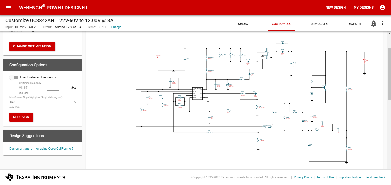
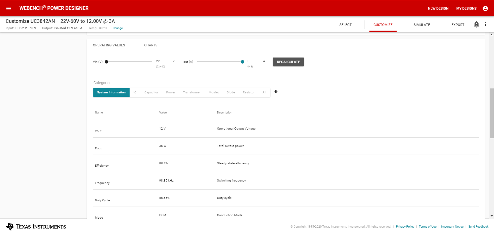
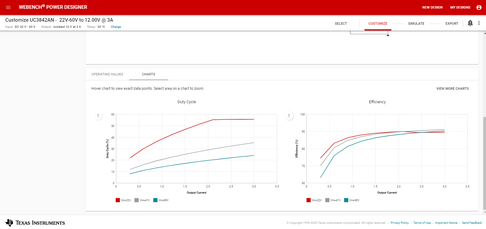
テキサス・インスツルメンツのWebench Power Designツールを使用して、類似の設計、特に回路仕様を検索する。このツールでは、回路図や各部品の特性のほか、電圧、電流、動作モード、部品の電力、回路線などのパラメータが用意されており、入力値を変更することもできる。
Simulation by SIMtrix / SIMPLIS software.
Simulate with input voltage: Vin = 22V, load : 100mA.
Simulate with input voltage: Vin = 22V, load : 3A.
Simulate with input voltage: Vin = 60V, load : 3A.
シミュレーション結果:
- Vin < 31VDC かつ Io < 2.3A のとき、回路は DCM モードで動作し、Io > 2.3A のとき、CCM モードで動作する。
- Vin>31VDCの場合、回路はDCMモードでのみ動作する。
同メーカーの類似設計のデータと比較すると、ほぼ同じ値である。
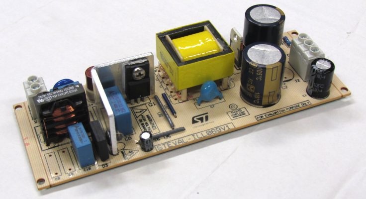
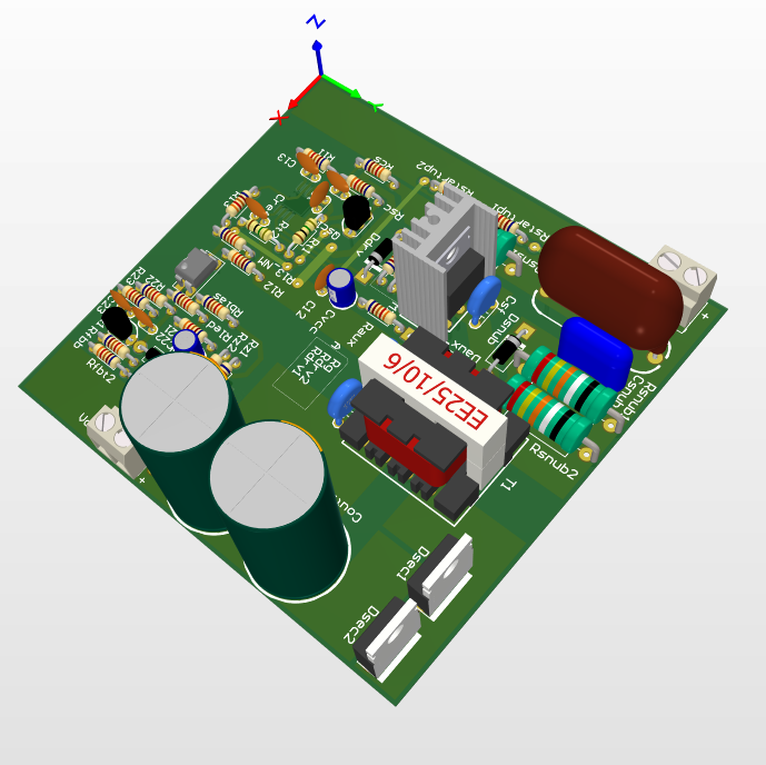
試作と評価
シミュレーション後、PCBレイアウト設計をして、組み立てた。
Measure and evaluate.
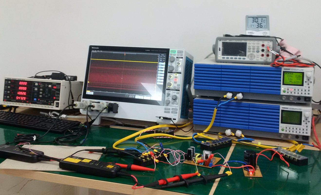
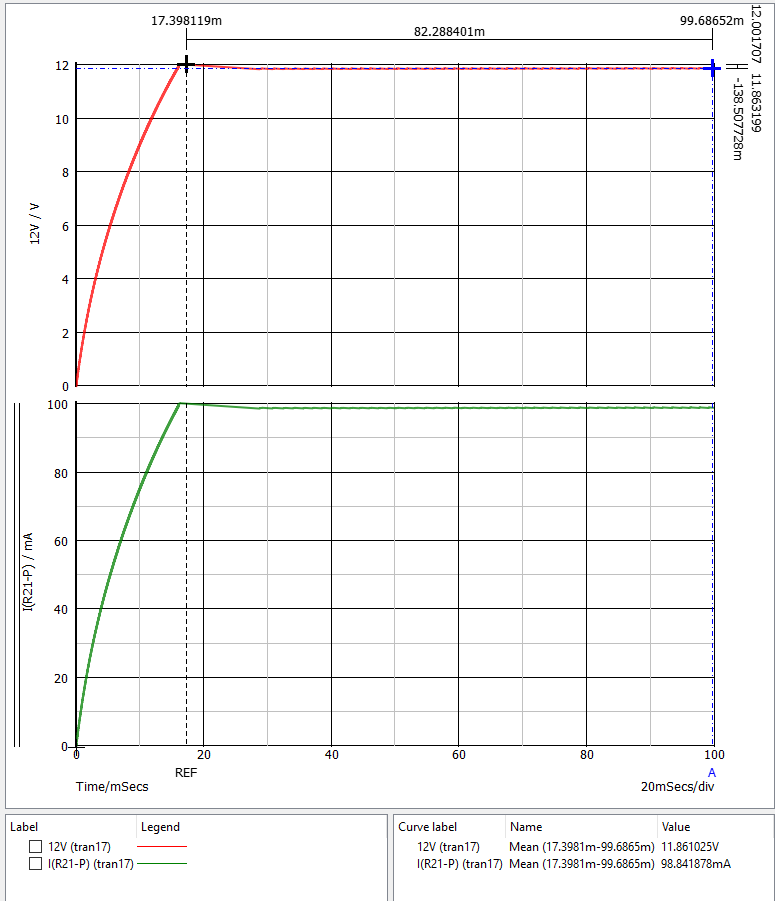
入出力 評価結果:
-
入出力仕様と測定結果:
| I_out ( A ) |
Output Voltage V_out (V) |
Total output power P_out (W) |
Input Current I_in (A) |
Duty cycle D (%) |
||||||||
| Input Voltage | Input Voltage | Input Voltage | Input Voltage | |||||||||
| 22 V | 41 V | 60 V | 22 V | 41 V | 60 V | 22 V | 41 V | 60 V | 22 V | 41 V | 60 V | |
0.1 |
11.99 |
11.98 |
11.99 |
1.20 |
1.20 |
1.20 |
0.14 |
0.09 |
0.08 |
27.13% |
14.16% |
12.20% |
0.2 |
11.98 |
11.98 |
11.98 |
2.40 |
2.40 |
2.40 |
0.21 |
0.13 |
0.11 |
29.35% |
15.70% |
14.48% |
0.3 |
11.98 |
11.98 |
11.98 |
3.59 |
3.59 |
3.59 |
0.28 |
0.17 |
0.13 |
32.44% |
16.42% |
15.57% |
0.4 |
11.97 |
11.97 |
11.98 |
4.79 |
4.79 |
4.79 |
0.35 |
0.20 |
0.16 |
34.04% |
17.09% |
16.46% |
0.5 |
11.97 |
11.97 |
11.97 |
5.99 |
5.98 |
5.99 |
0.42 |
0.24 |
0.18 |
39.52% |
18.61% |
17.78% |
0.6 |
11.97 |
11.97 |
11.97 |
7.18 |
7.18 |
7.18 |
0.49 |
0.28 |
0.21 |
41.87% |
19.78% |
18.83% |
0.7 |
11.96 |
11.96 |
11.97 |
8.37 |
8.37 |
8.38 |
0.56 |
0.31 |
0.24 |
43.87% |
21.36% |
19.07% |
0.8 |
11.96 |
11.96 |
11.96 |
9.57 |
9.57 |
9.57 |
0.63 |
0.35 |
0.26 |
45.35% |
22.40% |
20.09% |
0.9 |
11.96 |
11.96 |
11.96 |
10.76 |
10.76 |
10.76 |
0.71 |
0.39 |
0.29 |
47.83% |
22.80% |
20.43% |
1.0 |
11.95 |
11.95 |
11.95 |
11.95 |
11.95 |
11.95 |
0.78 |
0.43 |
0.31 |
49.31% |
23.92% |
20.47% |
1.2 |
11.94 |
11.94 |
11.95 |
14.33 |
14.33 |
14.34 |
0.93 |
0.50 |
0.36 |
51.10% |
26.95% |
21.84% |
1.4 |
11.94 |
11.94 |
11.94 |
16.71 |
16.71 |
16.72 |
1.09 |
0.58 |
0.41 |
53.19% |
29.34% |
22.61% |
1.6 |
11.93 |
11.93 |
11.93 |
19.09 |
19.09 |
19.09 |
1.25 |
0.65 |
0.46 |
54.96% |
31.30% |
23.48% |
1.8 |
11.92 |
11.92 |
11.93 |
21.46 |
21.46 |
21.47 |
1.42 |
0.73 |
0.51 |
56.85% |
32.08% |
24.59% |
2.0 |
11.92 |
11.92 |
11.92 |
23.83 |
23.83 |
23.84 |
1.62 |
0.81 |
0.57 |
57.85% |
34.31% |
25.47% |
2.2 |
11.90 |
11.91 |
11.91 |
26.19 |
26.20 |
26.20 |
1.85 |
0.89 |
0.62 |
58.85% |
36.24% |
26.38% |
2.4 |
11.89 |
11.90 |
11.90 |
28.54 |
28.56 |
28.57 |
1.88 |
0.97 |
0.67 |
58.83% |
37.47% |
27.67% |
2.6 |
11.89 |
11.89 |
11.90 |
30.90 |
30.92 |
30.93 |
1.91 |
1.05 |
0.73 |
58.83% |
41.38% |
28.13% |
2.8 |
11.88 |
11.88 |
11.89 |
33.25 |
33.28 |
33.29 |
1.95 |
1.15 |
0.79 |
58.86% |
42.00% |
29.01% |
2.9 |
11.87 |
11.88 |
11.89 |
34.41 |
34.45 |
34.47 |
2.04 |
1.23 |
0.84 |
58.85% |
42.12% |
30.18% |
3.0 |
11.84 |
11.81 |
11.88 |
35.53 |
35.43 |
35.65 |
2.06 |
1.26 |
0.90 |
58.85% |
42.18% |
31.10% |
-
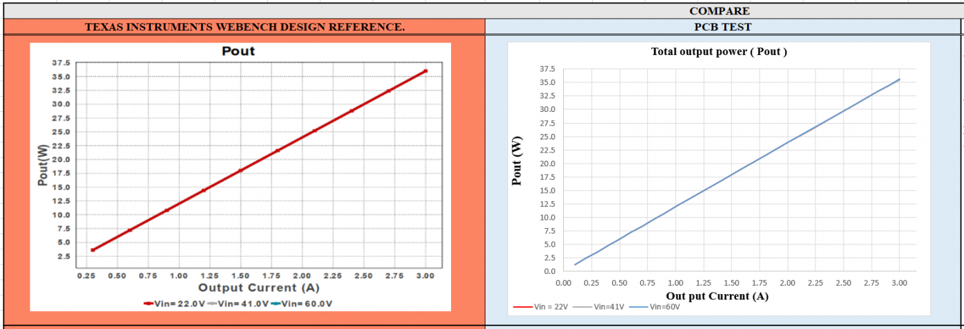
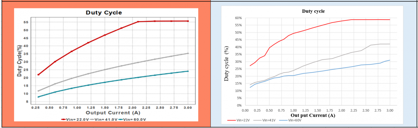
Webench Power Designでシミュレーションした特性と実測値の比較:
-
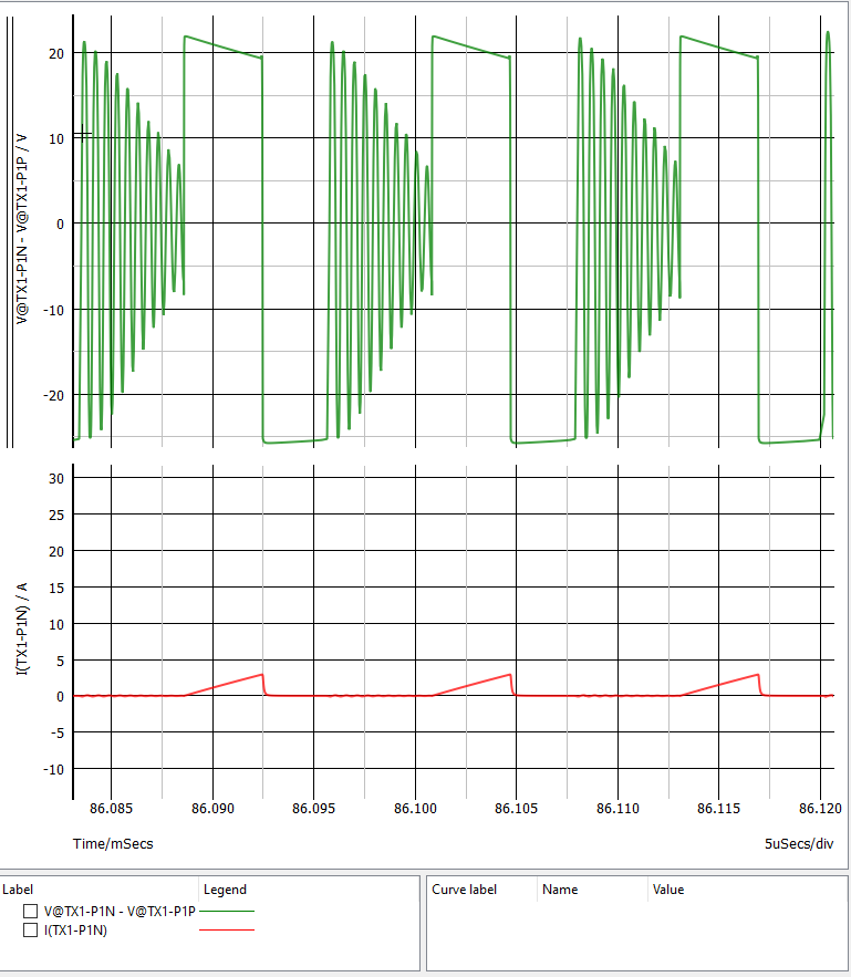
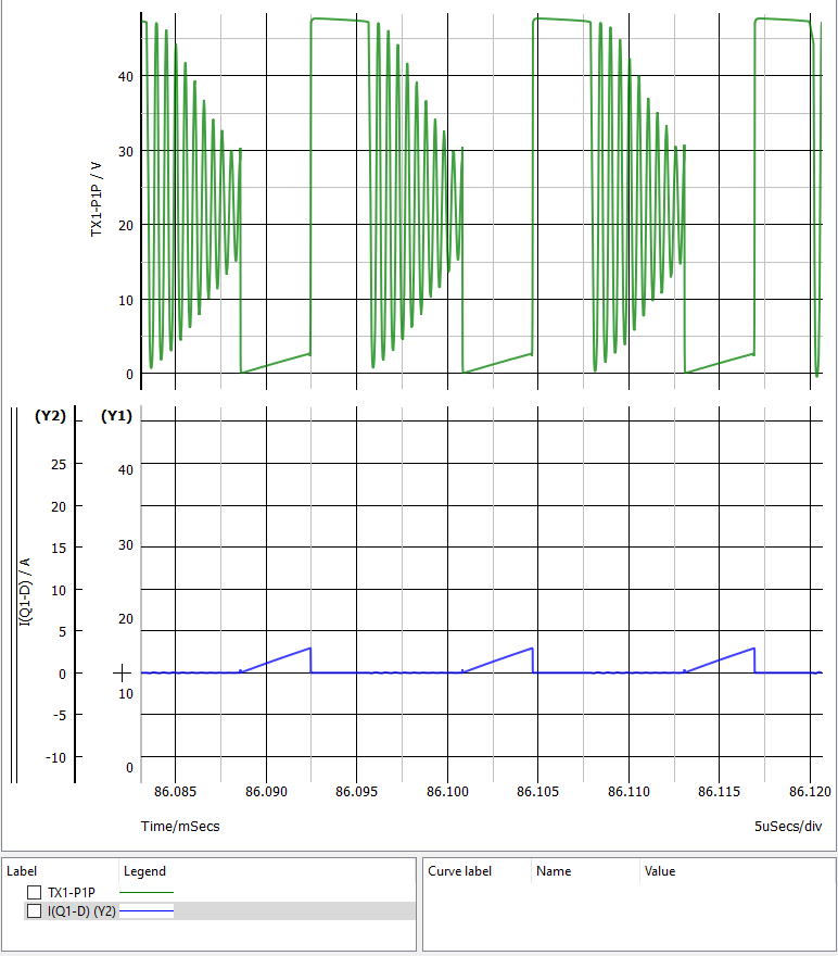
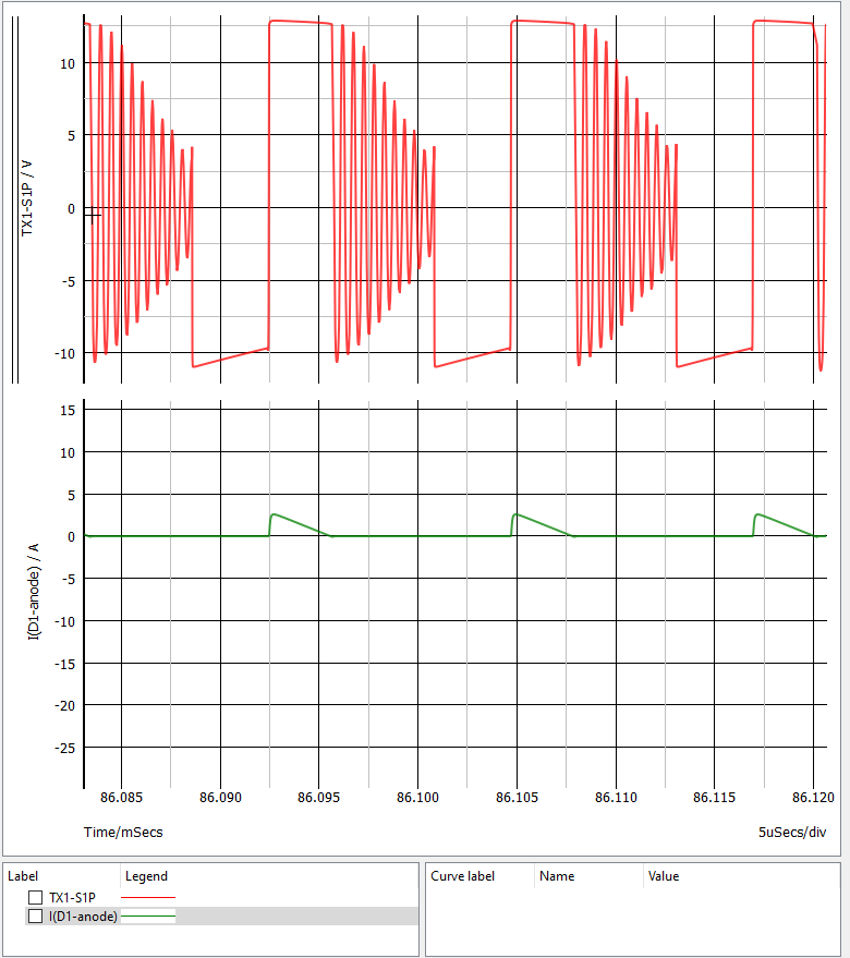
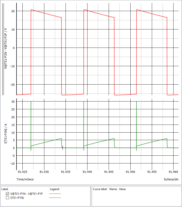
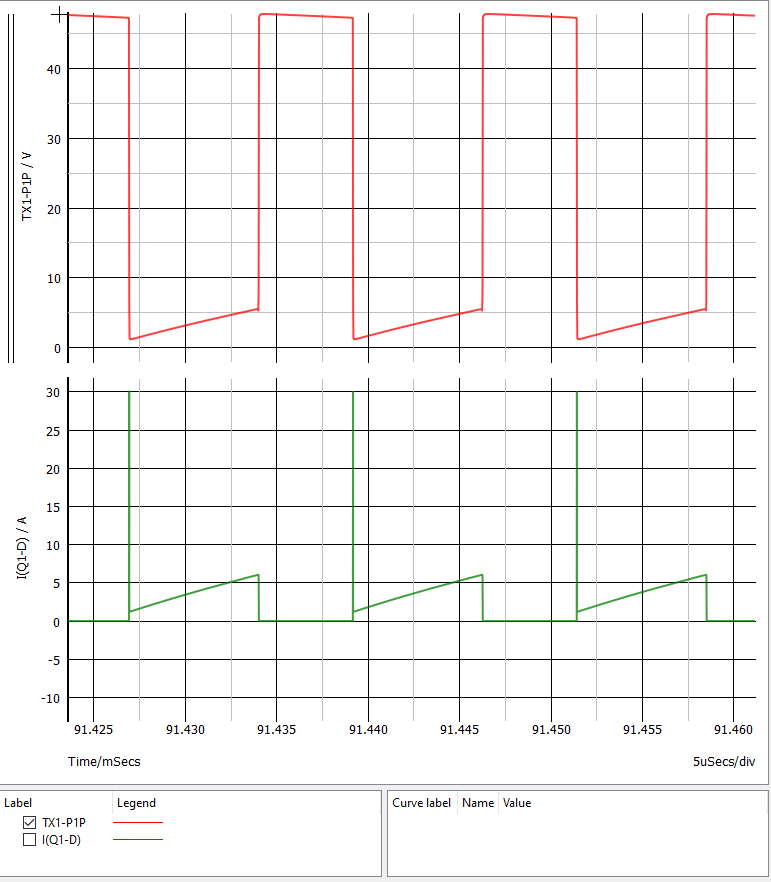
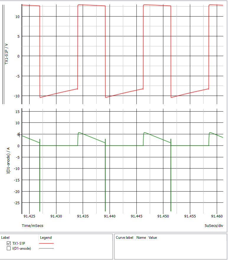
波形
トランス, MOSFET, 整流ダイオード 特性評価:
-
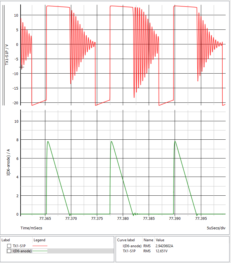
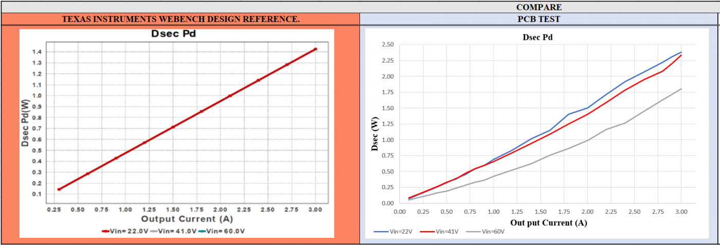
整流ダイオード電圧、電流測定結果:
| Iout ( A ) | Dsec If | Dsec Vf | Dsec Pd | Dsec If | Dsec Vf | Dsec Pd | Dsec If | Dsec Vf | Dsec Pd |
| 0.1 | 0.12237 | 0.58 | 0.070975 | 0.14025 | 0.585 | 0.082046 | 0.1581 | 0.33 | 0.052173 |
| 0.2 | 0.2229 | 0.6 | 0.13374 | 0.2375 | 0.595 | 0.141313 | 0.2542 | 0.35 | 0.08897 |
| 0.3 | 0.3214 | 0.605 | 0.194447 | 0.3367 | 0.61 | 0.205387 | 0.3538 | 0.35 | 0.12383 |
| 0.4 | 0.4166 | 0.62 | 0.258292 | 0.4359 | 0.61 | 0.265899 | 0.4529 | 0.36 | 0.163044 |
| 0.5 | 0.5179 | 0.62 | 0.321098 | 0.5368 | 0.61 | 0.327448 | 0.5506 | 0.35 | 0.19271 |
| 0.6 | 0.6207 | 0.63 | 0.391041 | 0.6332 | 0.61 | 0.386252 | 0.6486 | 0.365 | 0.236739 |
| 0.7 | 0.7182 | 0.63 | 0.452466 | 0.736 | 0.635 | 0.46736 | 0.7483 | 0.375 | 0.280612 |
| 0.8 | 0.8185 | 0.66 | 0.54021 | 0.8336 | 0.65 | 0.54184 | 0.8508 | 0.385 | 0.327558 |
| 0.9 | 0.9216 | 0.645 | 0.594432 | 0.9315 | 0.64 | 0.59616 | 0.948 | 0.385 | 0.36498 |
| 1 | 1.0257 | 0.67 | 0.687219 | 1.0334 | 0.635 | 0.656209 | 1.0518 | 0.4 | 0.42072 |
| 1.2 | 1.2232 | 0.685 | 0.837892 | 1.2292 | 0.65 | 0.79898 | 1.2453 | 0.42 | 0.523026 |
| 1.4 | 1.4241 | 0.715 | 1.018232 | 1.4283 | 0.66 | 0.942678 | 1.4446 | 0.43 | 0.621178 |
| 1.6 | 1.6212 | 0.71 | 1.151052 | 1.6295 | 0.67 | 1.091765 | 1.6451 | 0.46 | 0.756746 |
| 1.8 | 1.8732 | 0.75 | 1.4049 | 1.8336 | 0.68 | 1.246848 | 1.8433 | 0.47 | 0.866351 |
| 2 | 2.069 | 0.725 | 1.500025 | 2.0319 | 0.69 | 1.402011 | 2.0423 | 0.485 | 0.990515 |
| 2.2 | 2.272 | 0.755 | 1.71536 | 2.274 | 0.7 | 1.5918 | 2.285 | 0.51 | 1.16535 |
| 2.4 | 2.473 | 0.775 | 1.916575 | 2.472 | 0.72 | 1.77984 | 2.482 | 0.51 | 1.26582 |
| 2.6 | 2.669 | 0.776 | 2.071144 | 2.669 | 0.73 | 1.94837 | 2.684 | 0.54 | 1.44936 |
| 2.8 | 2.873 | 0.774 | 2.223702 | 2.871 | 0.725 | 2.081475 | 2.884 | 0.565 | 1.62946 |
| 2.9 | 2.965 | 0.778 | 2.30677 | 2.973 | 0.74 | 2.20002 | 2.983 | 0.575 | 1.715225 |
| 3 | 3.043 | 0.782 | 2.379626 | 3.073 | 0.76 | 2.33548 | 3.086 | 0.585 | 1.80531 |
- 実測値とWebench Power Designの比較:
- 波形
-
-
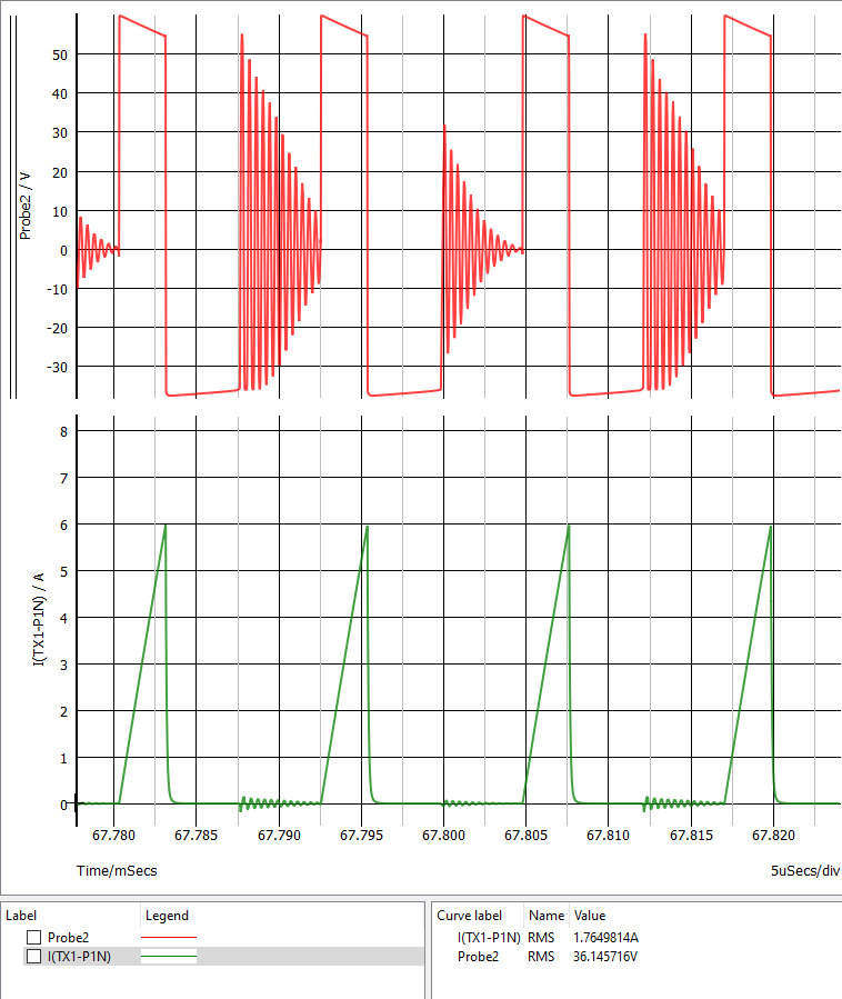
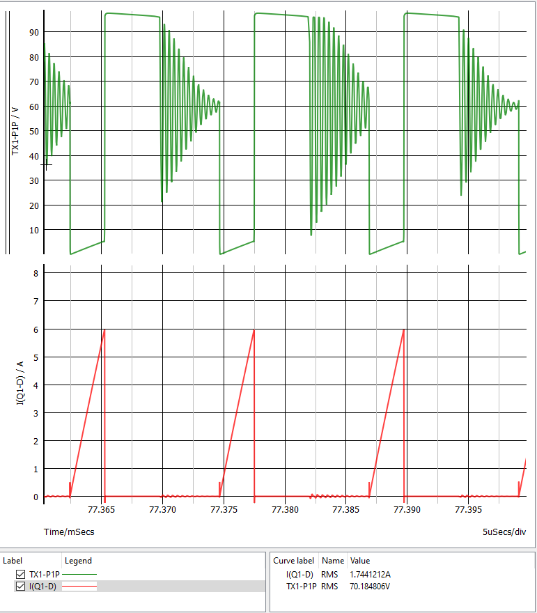
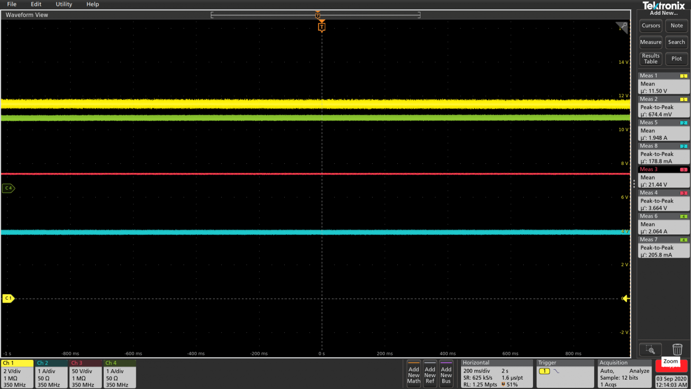
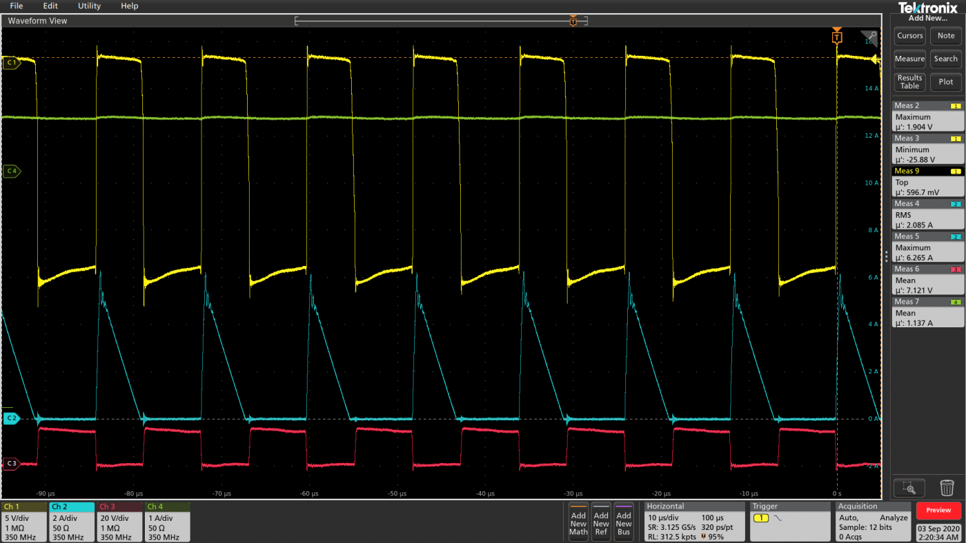
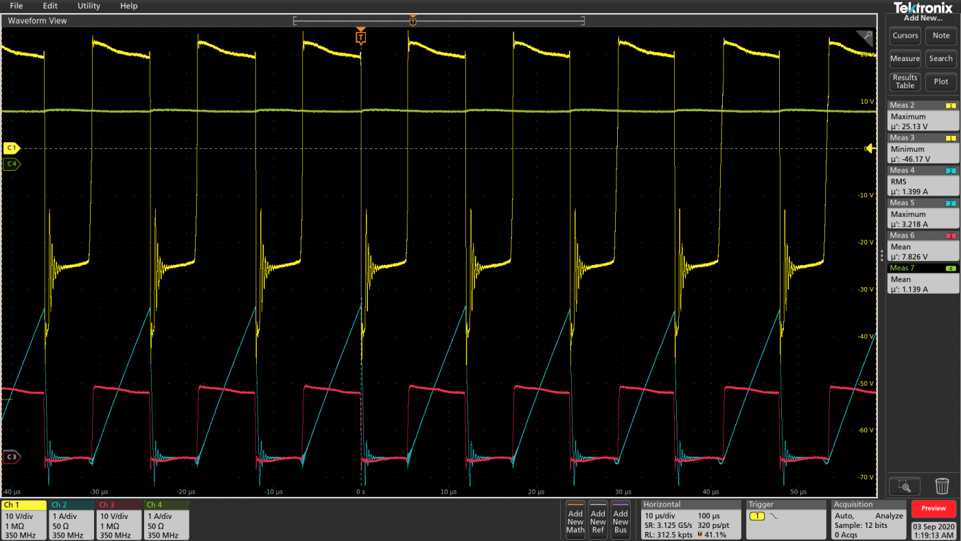
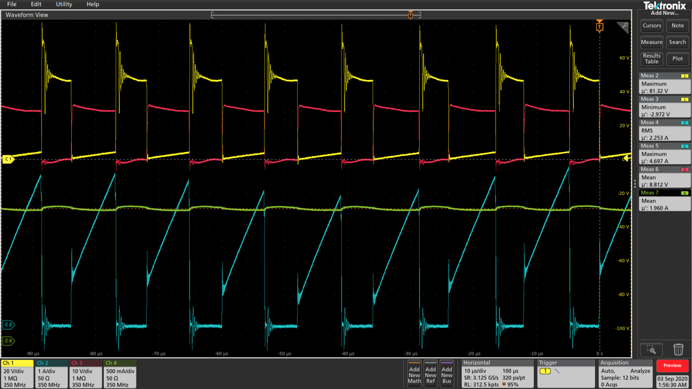
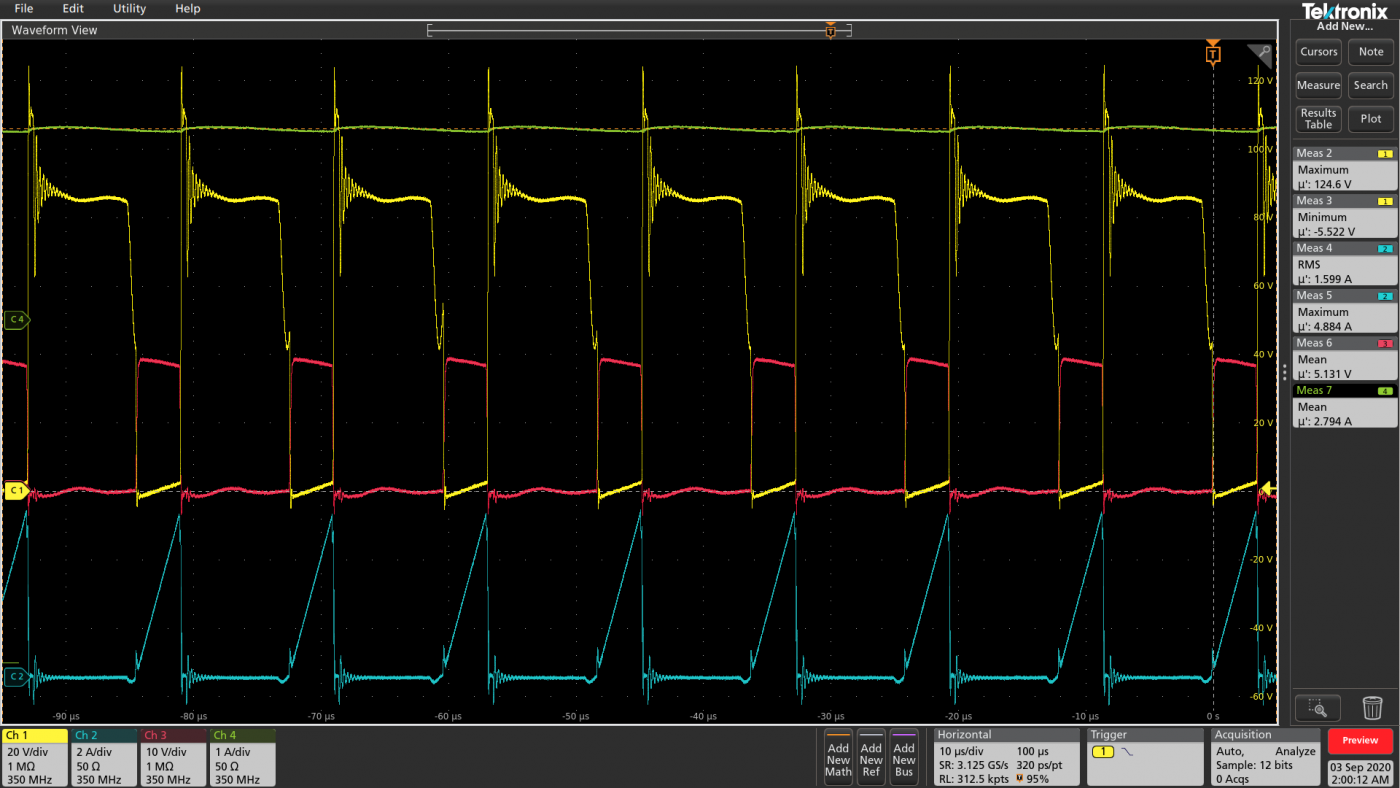
測定結果 入力電圧: Vin = 22V, load Io = 1.1 A. 回路は DCM modeで動作している。:
-
-
-
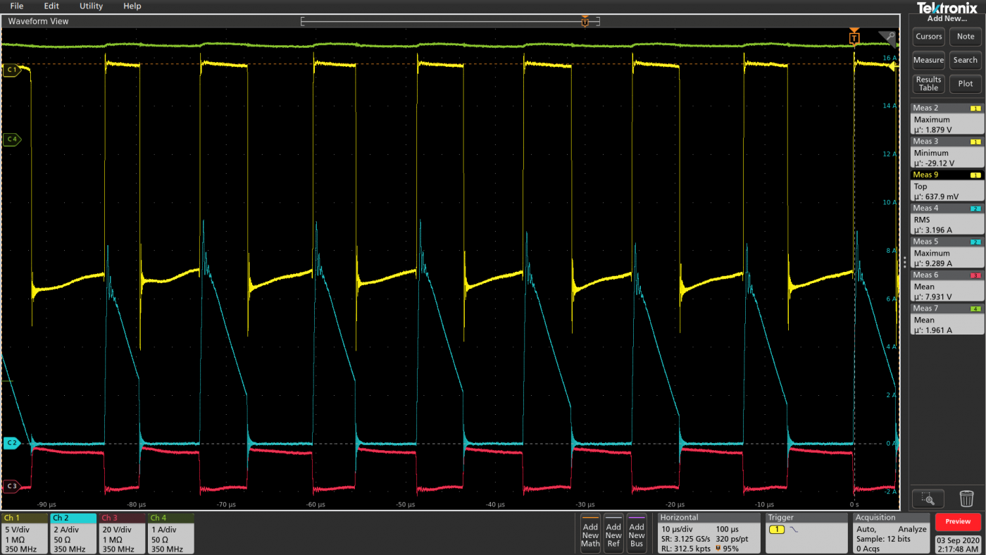
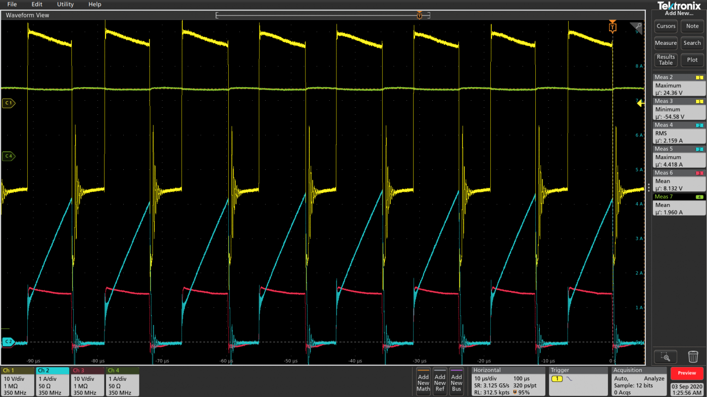
測定結果 入力電圧: Vin = 22V, load Io = 1.961 A. 回路は CCM modeで動作している。:
-
-
-
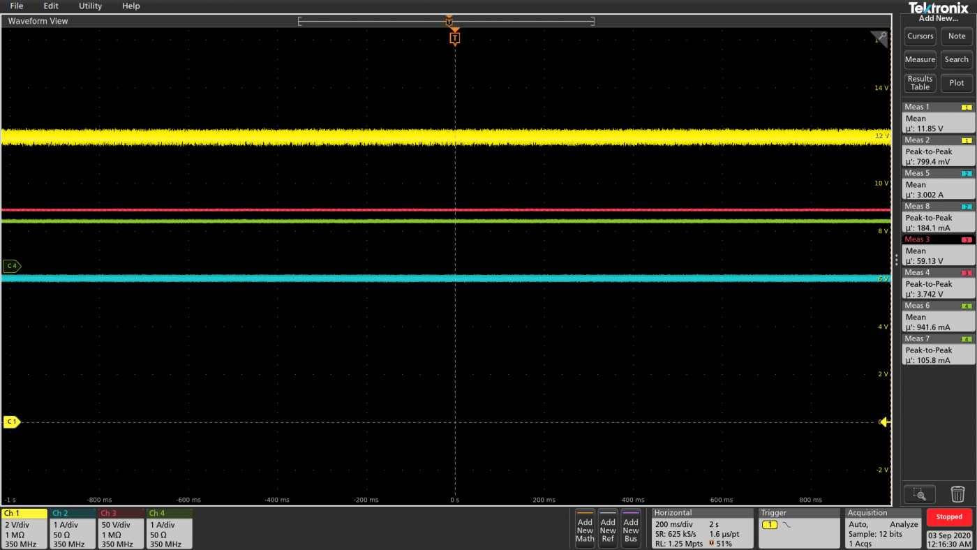
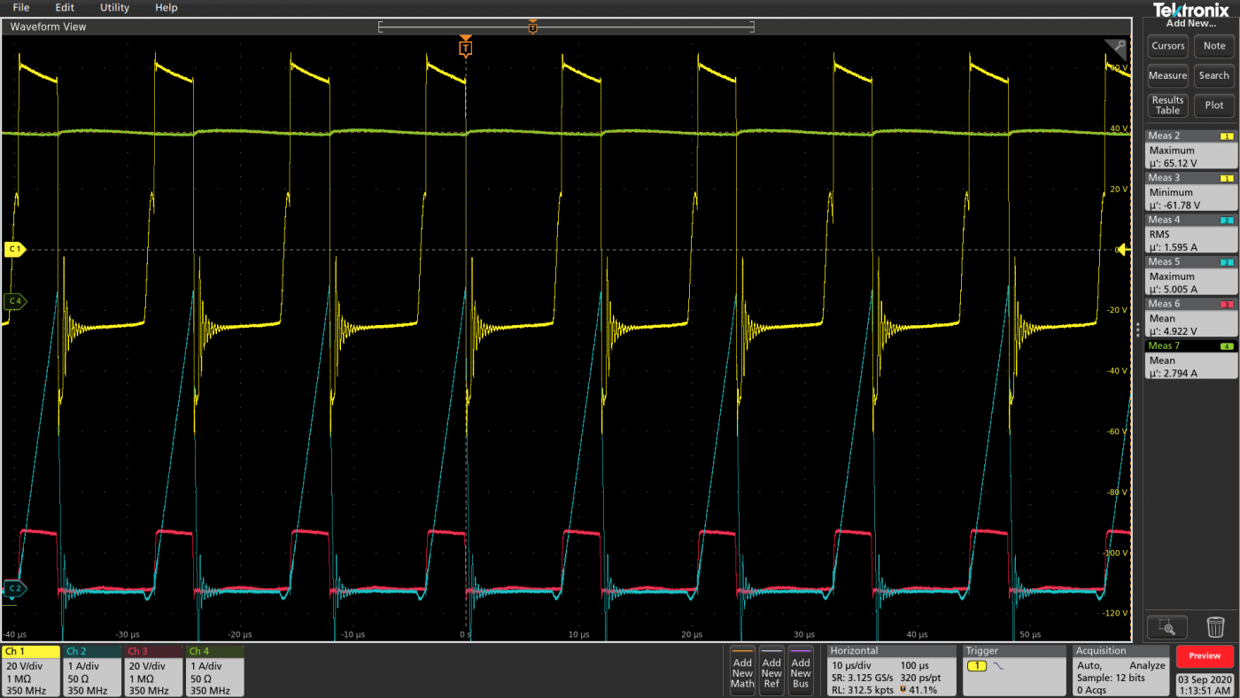
測定結果 入力電圧: Vin = 60V, load Io = 2.8 A. 回路は DCM modeで動作している。:
-

-
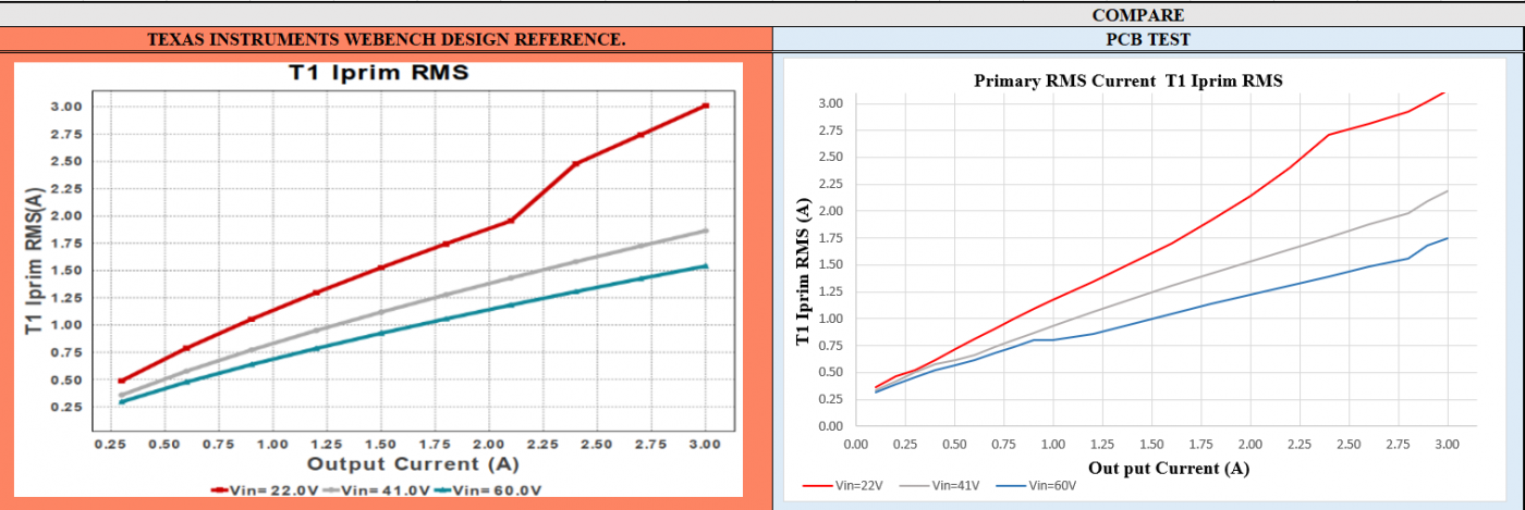
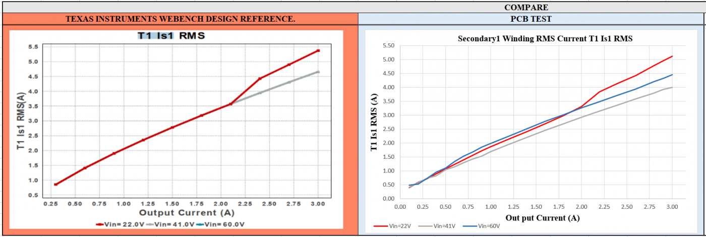
1次側実効電流、二次側実効電流測定結果:
| Iout ( A ) | Primary RMS Current T1 Iprim RMS (A) |
Secondary1 Winding RMS Current T1 Is1 RMS (A) |
||||
| Input Voltage | Input Voltage | |||||
| 22 V | 41 V | 60 V | 22 V | 41 V | 60 V | |
| 0.1 | 0.3682 | 0.3331 | 0.3216 | 0.3902 | 0.4102 | 0.4802 |
| 0.2 | 0.4622 | 0.4235 | 0.3928 | 0.5887 | 0.5661 | 0.5312 |
| 0.3 | 0.5208 | 0.5060 | 0.4570 | 0.7205 | 0.7331 | 0.7370 |
| 0.4 | 0.6202 | 0.5753 | 0.5236 | 0.8983 | 0.8250 | 0.9550 |
| 0.5 | 0.7161 | 0.6177 | 0.5700 | 1.0700 | 1.0400 | 1.1030 |
| 0.6 | 0.8114 | 0.6636 | 0.6165 | 1.2350 | 1.1520 | 1.3370 |
| 0.7 | 0.9072 | 0.7339 | 0.6813 | 1.3960 | 1.2880 | 1.5330 |
| 0.8 | 0.9983 | 0.8025 | 0.7405 | 1.5650 | 1.4270 | 1.6720 |
| 0.9 | 1.0900 | 0.8663 | 0.7992 | 1.7170 | 1.5330 | 1.8540 |
| 1.0 | 1.1800 | 0.9312 | 0.8035 | 1.8630 | 1.6860 | 1.9820 |
| 1.2 | 1.3500 | 1.0610 | 0.8571 | 2.1420 | 1.9510 | 2.2500 |
| 1.4 | 1.5230 | 1.1870 | 0.9545 | 2.4130 | 2.2060 | 2.5200 |
| 1.6 | 1.7050 | 1.3040 | 1.0460 | 2.6960 | 2.4520 | 2.7760 |
| 1.8 | 1.9120 | 1.4190 | 1.1380 | 2.9910 | 2.6870 | 3.0220 |
| 2.0 | 2.1440 | 1.5370 | 1.2260 | 3.3080 | 2.9260 | 3.2640 |
| 2.2 | 2.4040 | 1.6460 | 1.3060 | 3.8410 | 3.1490 | 3.4910 |
| 2.4 | 2.7150 | 1.7570 | 1.3960 | 4.1552 | 3.3710 | 3.7210 |
| 2.6 | 2.8151 | 1.8780 | 1.4830 | 4.4338 | 3.5960 | 3.9460 |
| 2.8 | 2.9292 | 1.9820 | 1.5630 | 4.7825 | 3.8010 | 4.2100 |
| 2.9 | 3.0192 | 2.0890 | 1.6790 | 4.9530 | 3.9320 | 4.3190 |
| 3.0 | 3.1256 | 2.1920 | 1.7490 | 5.1254 | 4.0000 | 4.4550 |
- Webench Power Designシミュレーション結果と実測値比較:
- 波形
-
-
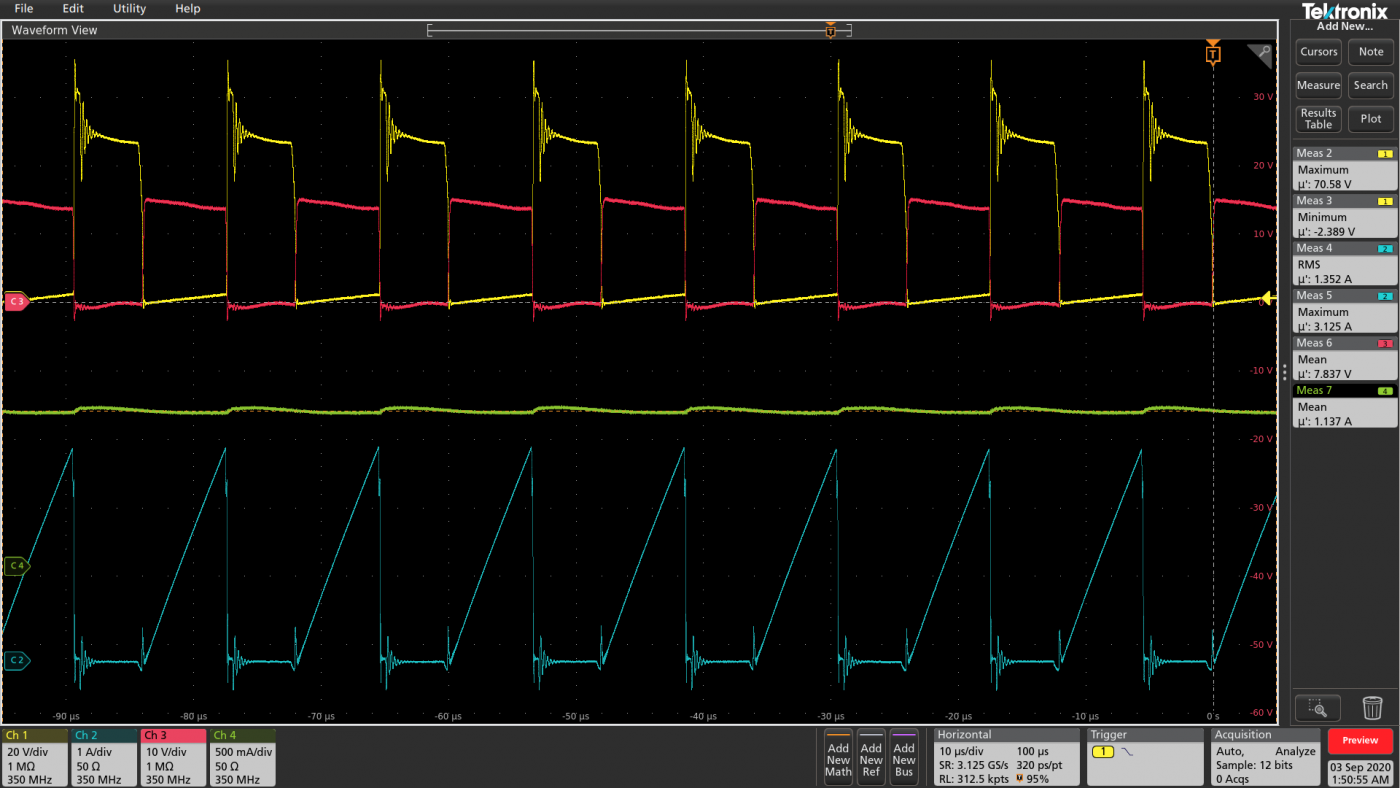
測定結果 入力電圧: Vin = 22V, load Io = 1.1 A. 回路は DCM modeで動作している。
-
-
-
測定結果 入力電圧: Vin = 22V, load Io = 1.9611 A. 回路は CCM modeで動作している。
-
-
-
-
測定結果 入力電圧: Vin = 60V, load Io = 2.8 A. 回路は DCM modeで動作している。
-
-
MOSFET specifications evaluation:
-
Waveform.
-
測定結果 入力電圧: Vin = 22V, load Io = 1.1 A. 回路は DCM modeで動作している。
-
-
-
測定結果 入力電圧: Vin = 22V, load Io = 1.961 A. 回路は CCM modeで動作している。
-
-
-
測定結果 入力電圧: Vin = 60V, load Io = 2.8 A. 回路は DCM modeで動作している。
-
研究の過程では、欠点があることは避けられませんが、読者の皆さんからコメントをいただき、改善に役立てたいと考えています。
ARV-DN Team
References:
Markus Zehendner, Matthias Ulmann, “Power Topologies Handbook “, Texas Instruments.
“Under the Hood of Flyback SMPS Designs”, TI Literature Number: SLUP254,Texas Instruments.
“Methods of Designing PWM Flyback Converter”, Rohm Semiconductor.
“Design Guidelines for RCD Snubber of Flyback Converters”, Application Note AN-4147, Fairchild Semiconductor.
“DC-DC Converters Feedback and Control”, Application Note TND352, ON Semiconductor
https://webench.ti.com/power-designer/switching-regulator